
High energy beam polysilicon purifying device

A technology of polysilicon and high-energy beams, which is applied in the direction of silicon compounds, inorganic chemistry, non-metallic elements, etc., can solve problems such as high cost, large energy consumption, and environmental pollution

Inactive Publication Date: 2010-06-16
BEIHANG UNIV
View PDF5 Cites 0 Cited by
  • Summary
  • Abstract
  • Description
  • Claims
  • Application Information

AI Technical Summary

Problems solved by technology

It solves the defects of large investment, high cost, large energy consumption and serious environmental pollution in the current production of solar grade silicon by chemical method

Method used


Image

  • High energy beam polysilicon purifying device
  • High energy beam polysilicon purifying device
  • High energy beam polysilicon purifying device

Examples


Embodiment Construction

[0020] The present invention will be further described in detail below in conjunction with the accompanying drawings.

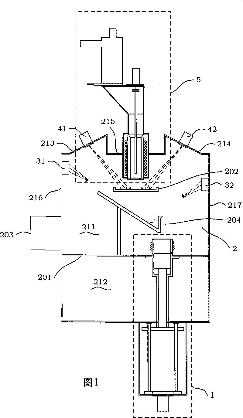
[0021] Referring to Fig. 1, the present invention is a four-in-one high-energy beam polysilicon purification device integrating isovacuum electromagnetic induction smelting, electron beam smelting, ion smelting, and directional solidification. The purification device includes a directional solidification unit 1, a vacuum Chamber 2, plasma smelting unit, electron beam smelting unit, vacuum electromagnetic induction smelting unit 5; vacuum electromagnetic induction smelting unit 5 is installed on the concave surface 215 of vacuum chamber 2; A electron gun 41 of electron beam smelting unit is installed in vacuum chamber 2 On the left inclined plane 213 of the vacuum chamber 2, the B electron gun 42 is installed on the right inclined plane 214 of the vacuum chamber 2; On the right housing 217 ; the connection seat 182 of the directional solidification unit 1 is i...


PUM

PropertyMeasurementUnit
diameteraaaaaaaaaa

Abstract

The invention discloses a device for purifying polysilicon by using a high energy beam, comprising a vacuum chamber, a vacuum electromagnetic induction smelting unit, an electron beam smelting unit, aplasma smelting unit and a directional solidification unit. The vacuum electromagnetic induction smelting unit is arranged on a concave surface of the vacuum chamber; an A electron gun of the electron beam smelting unit is arranged on a left inclined plane of the vacuum chamber and a B electron gun is arranged on a right inclined plane of the vacuum chamber; an A plasma gun of the plasma smeltingunit is arranged on a left shell body of the vacuum chamber and a B plasma gun is arranged on a right shell body of the vacuum chamber; a connecting base of the directional solidification unit is arranged on a separator of the vacuum chamber; the invention aims at providing a device for purifying the polysilicon by using the high energy beam which integrates four technologies of the vacuum electromagnetic induction smelting, the plasma smelting, the electron beam smelting and the directional solidification; the purifying device carries out vacuum electromagnetic induction smelting, plasma smelting, electron beam smelting and directional solidification sequentially for silicon metal of 99.9 percent to obtain the polysilicon with a purity of 99.9999 percent which is used for producing solarbatteries. The invention solves the defects of large equipment input, high cost, large energy consumption and serious environmental pollution in the prior chemical methods for producing solar grade silicon.

Description

technical field [0001] The invention relates to a kind of equipment for purifying metal and non-metal materials, more specifically, it refers to a high-energy beam polysilicon purification which integrates vacuum electromagnetic induction smelting, electron beam smelting, plasma smelting and directional solidification. device. Background technique [0002] The development and utilization of photovoltaic technology is an effective way to solve strategic problems such as global energy shortage and ecological environment deterioration. Polycrystalline silicon cells account for more than 60% of the world's total solar cell production. [0003] In 2005, the gap of high-purity polysilicon required by the global photovoltaic industry reached 24%, and the gap in my country was as high as 97%. The shortage of solar-grade polysilicon materials is the bottleneck restricting the solar photovoltaic industry. [0004] The existing production methods of solar grade silicon include chemic...

Claims


Application Information

Patent Timeline
Patent Type & Authority Patents(China)
IPC IPC(8): C01B33/037
Inventor 李合非宋连红逄广林徐惠彬
Owner BEIHANG UNIV
Learn More