Method for measuring nano-scale multilayer film structure
A measurement method and multi-layer film technology, which is applied in the field of optical measurement, can solve problems such as the difficulty in solving the diffusion film structure, and achieve the effect of avoiding easy to fall into local minimum
- Summary
- Abstract
- Description
- Claims
- Application Information
AI Technical Summary
Problems solved by technology
Method used
Image
Examples
Embodiment Construction
[0027] 1. A 40-period Mo / Si multilayer film was prepared on an ion beam sputtering coater, wherein the thickness of the Mo layer was 2.64nm, and the thickness of the Si layer was 3.96nm.
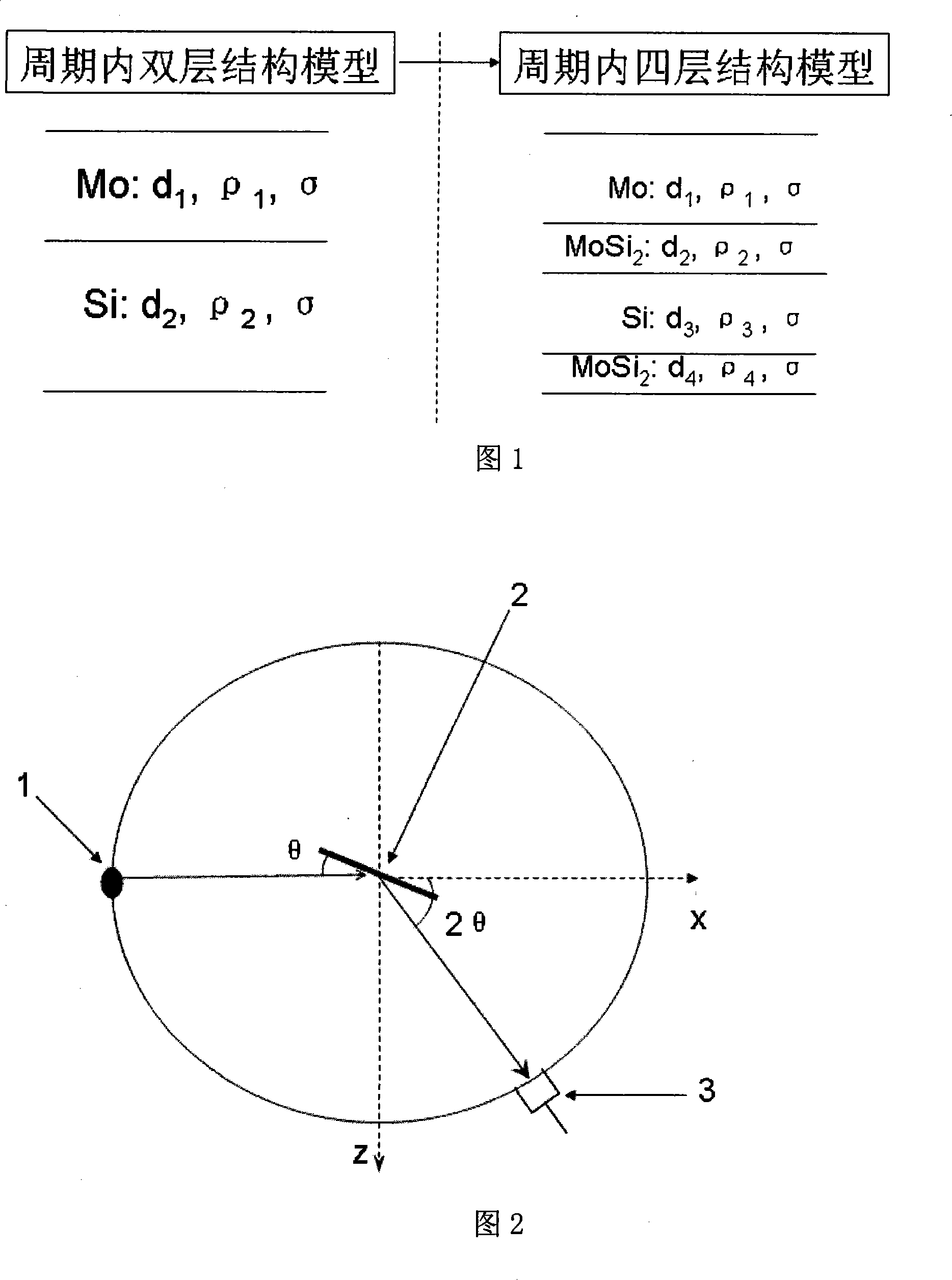
[0028] 2. Utilize the X-ray diffractometer to measure the grazing incidence reflectance R'=R'(θ) of the multilayer film, and the optical path is as shown in Figure 2. The X-ray wavelength is 0.154nm, the working mode is θ-2θ mode, the measurement angle range is θ: 0~5degree, and the scanning step is θ step =0.001degree, detector angular resolution: Δθ=0.016degree.
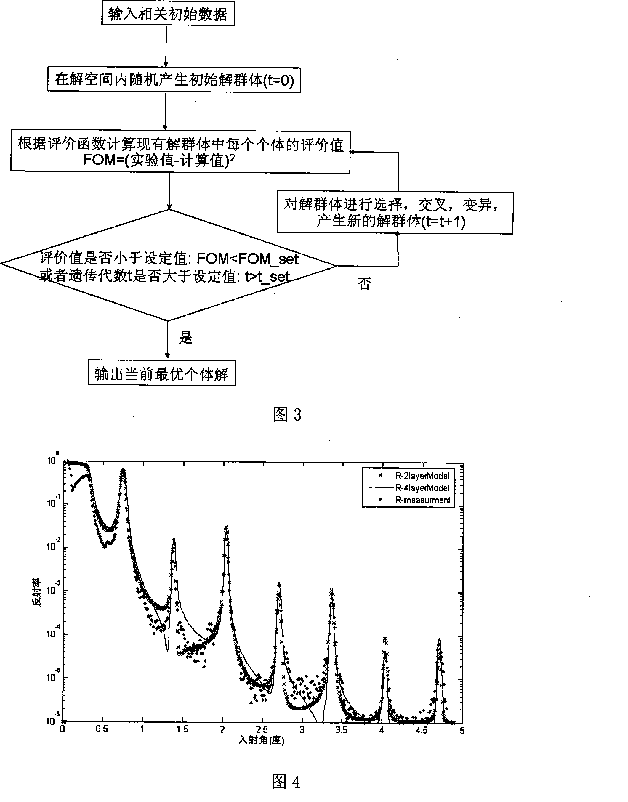
[0029] 3. Establish the four-layer structure model of the Mo / Si double-layer structure multilayer film [Mo / MoSi 2 / Si / MoSi 2 ], get the X-ray grazing incidence reflectance expression R=R(d1, d2, d3, d4, ρ1, ρ2, ρ3, ρ4, σ, θ) according to formula (1), establish as shown in formula (2) evaluation function. The evaluation function is fitted by a genetic algorithm, and the specific fitting process is shown in Figure 3. The first...
PUM
| Property | Measurement | Unit |
|---|---|---|
| wavelength | aaaaa | aaaaa |
Abstract
Description
Claims
Application Information
 - R&D
- Intellectual Property
- Life Sciences
- Materials
- Tech Scout
- Unparalleled Data Quality
- Higher Quality Content
- 60% Fewer Hallucinations
Browse by: Latest US Patents, China's latest patents, Technical Efficacy Thesaurus, Application Domain, Technology Topic, Popular Technical Reports.
© 2025 PatSnap. All rights reserved.Legal|Privacy policy|Modern Slavery Act Transparency Statement|Sitemap|About US| Contact US: help@patsnap.com


