No empty hole installation method for installing electronic components

A technology for electronic components and installation methods, which is applied in the direction of assembling printed circuits, electrical components, and electrical components with electrical components, and can solve problems such as crushing, difficulty in filling hollow areas, and lack of support at the bottom of electronic components.

Active Publication Date: 2008-04-30
TRIPOD WUXI ELECTRONICS
View PDF3 Cites 6 Cited by
  • Summary
  • Abstract
  • Description
  • Claims
  • Application Information

AI Technical Summary

Problems solved by technology

However, there is usually a recessed void area between the set of connection points. When the electronic component is mounted on the set of connection points, the electronic component is actually mounted on the void area, which leads to the subsequent lamination process. , it is extremely easy to be crushed due to the lack of complete support at the bottom of the electronic component
Although, in the existing technology, before the lamination process, the above-mentioned voids are filled with insulating materials as much as possible, but the three-dimensional obstacles caused by the electronic components themselves make it difficult to completely fill the voids

Method used


Image

  • No empty hole installation method for installing electronic components
  • No empty hole installation method for installing electronic components
  • No empty hole installation method for installing electronic components

Examples


Embodiment Construction

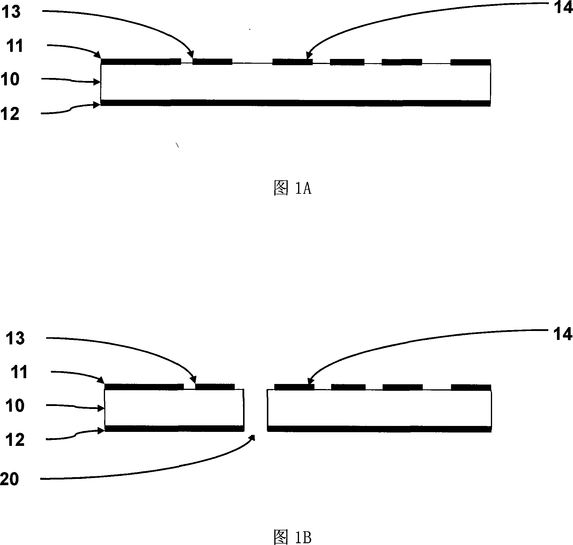
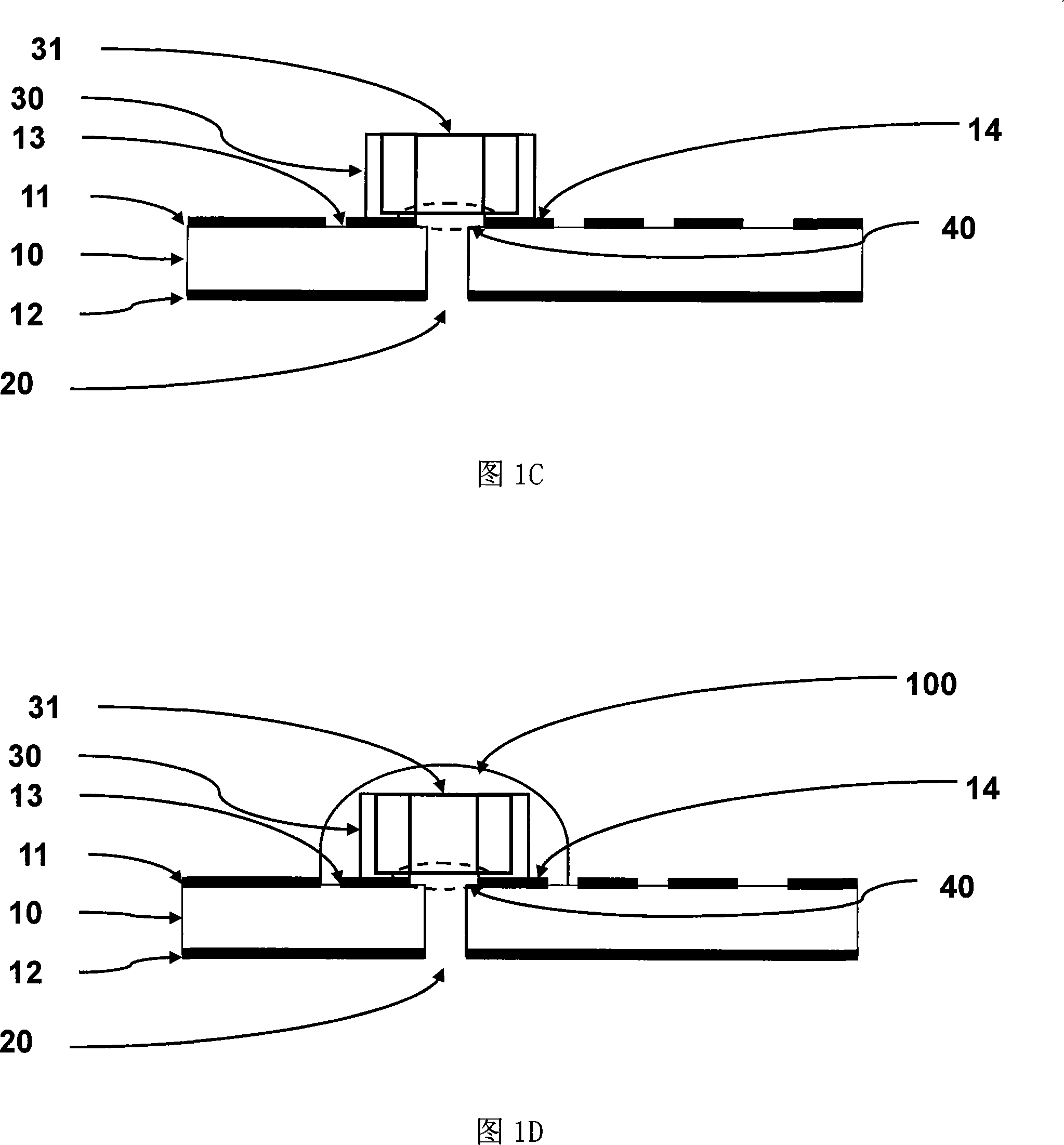
[0020] Please refer to FIGS. 1A to 1E. FIGS. 1A to 1E are schematic diagrams of a first implementation of a cavity-free mounting method for mounting electronic components of the present invention. As shown in Figure 1A, in order to make the circuit board (including the substrate 10, the circuit layer 11, and the power / ground layer 12) electrically connect to the electronic components 31 (such as passive components, capacitors, resistors or diodes), the circuit board A set of connection points will be made first. The set of connection points can be composed of two connection points 13,14.

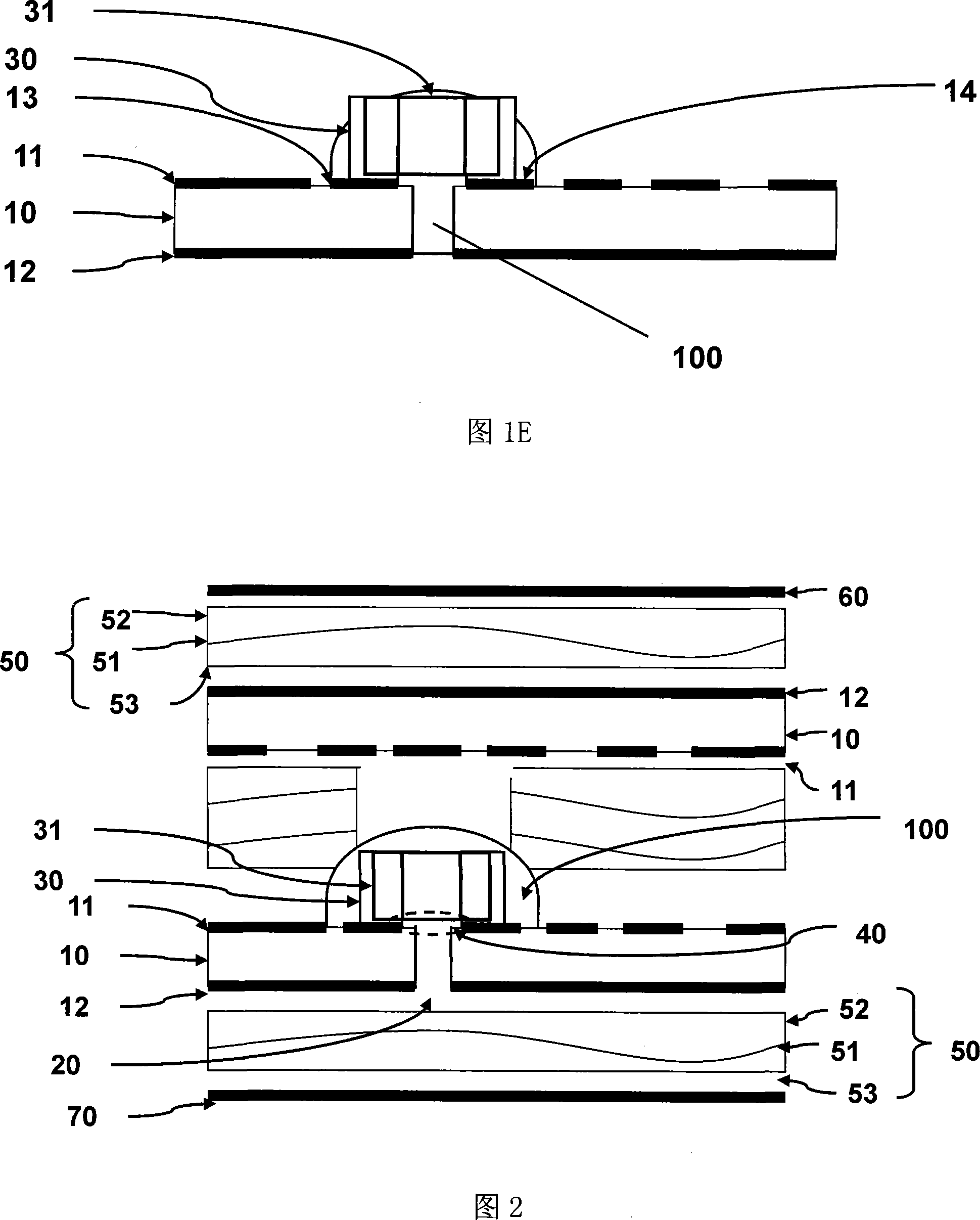
[0021] To put it simply, as shown in FIG. 1D, in order to provide complete support for the electronic component 31, the insulating material 100 is introduced through the electronic component 31 to the air guide hole 20 underneath the electronic component 31 by vacuum attraction, and filled with The cavity area 40 between the component 31 and a set of connection points 13 and 14. It should be not...


PUM


Abstract

In the void-free installation method for installing electronic components of the present invention, the insulating material originally applied on the electronic components is guided to the air guide holes between a group of connection points on the circuit board until at least the electronic components and the A hollow area between a set of connection points. In the void-free installation method for installing electronic components of the present invention, when the electronic components are assembled to a group of connection points on the circuit board, the insulating material that has been formed between the group of connection points in advance will be damaged by electrons. Compression of the component while filling the void area between the electronic component and a set of connection points.

Description

Technical field [0001] The invention relates to a method for embedding electronic components, in particular to a cavity-free installation method for installing electronic components. Background technique [0002] The so-called "embedded passive components" (Embedded Passives), is the use of the inner layer of the multilayer board process, etching or printing, the capacitor or resistor is directly made into the inner layer board, and then pressed into a multilayer After the board is installed, the discrete passive components welded during assembly on the board can be replaced, so as to save the board space to the active components and their wiring. [0003] Buried, implanted or concealed technology, Ohmega-ply first used the matt side of the original copper foil on the inner layer of the board, and processed the phosphor-nickel alloy layer on the thin film as resistive The components (Resistive Element) are pressed into a Thin core, and then two photoresist and three etching techn...

Claims


Application Information

Patent Timeline
IPC IPC(8): H05K13/04H05K3/30
Inventor 石汉青范字远谢子明
Owner TRIPOD WUXI ELECTRONICS
Why Eureka
Try Eureka