
Multi-order non-volatility memory and manufacturing method and operation method therefor

A non-volatile, method-of-operation technology, which is applied in static memory, read-only memory, semiconductor/solid-state device manufacturing, etc., can solve the problems of taking a long time and the distribution range of the initial voltage is small, so as to improve the erasing operation speed , save manufacturing cost, increase the effect of process margin

Inactive Publication Date: 2008-02-06
POWERCHIP SEMICON CORP
View PDF0 Cites 12 Cited by
  • Summary
  • Abstract
  • Description
  • Claims
  • Application Information

AI Technical Summary

Problems solved by technology

[0005] However, when the memory in the NOR type non-volatile memory is used as a multi-level memory cell, since the starting voltage distribution range for distinguishing each data state is small
In this way, in the programming operation of the existing NOR type non-volatile memory, it is necessary to perform multiple programming steps and programming confirmation steps, so that the programmed memory cells are accurately located in the set initial voltage distribution range, This will take a long time

Method used


Image

  • Multi-order non-volatility memory and manufacturing method and operation method therefor
  • Multi-order non-volatility memory and manufacturing method and operation method therefor
  • Multi-order non-volatility memory and manufacturing method and operation method therefor

Examples


Embodiment Construction

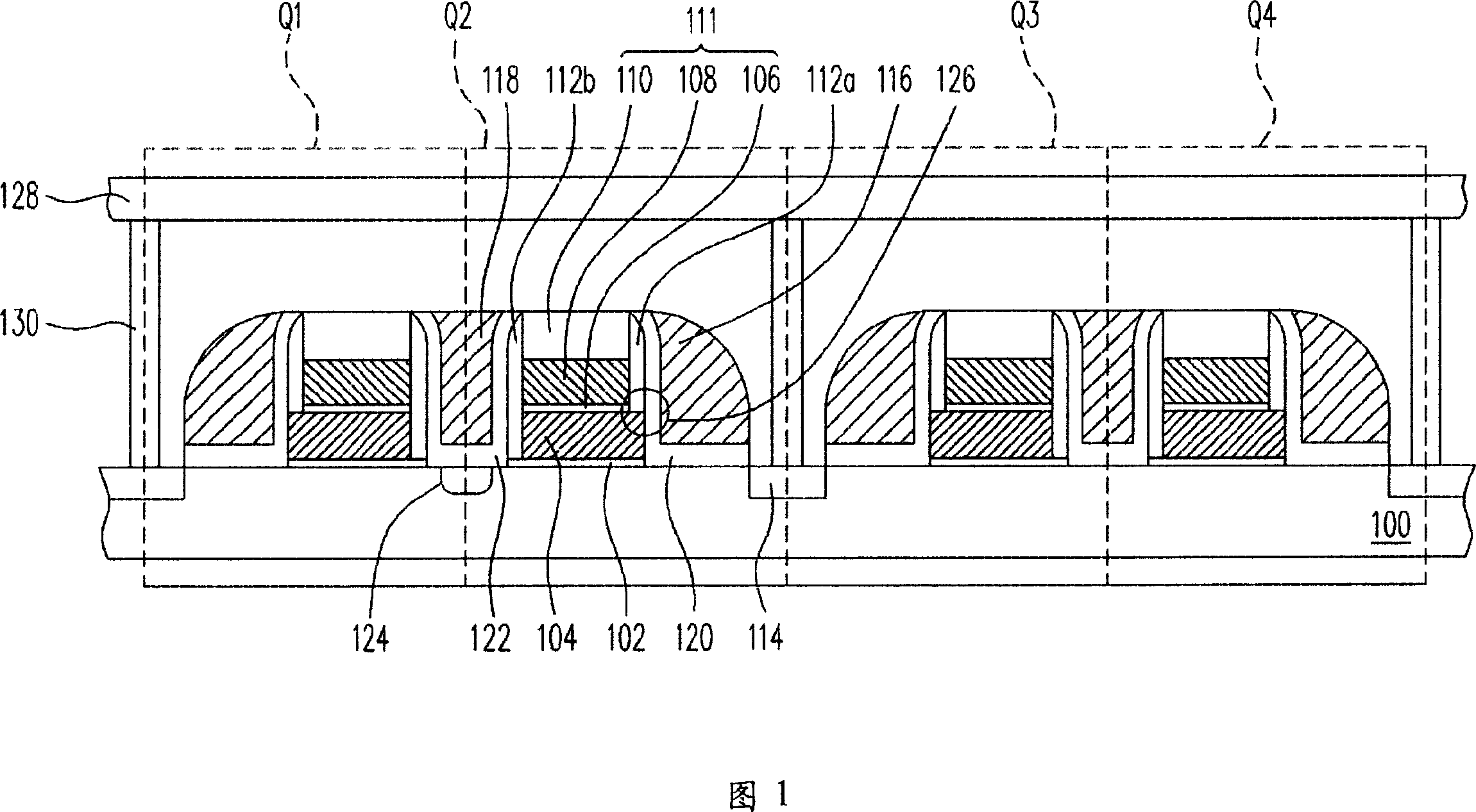
[0099] FIG. 1 is a cross-sectional view showing the structure of a non-volatile memory according to an embodiment of the present invention.

[0100] Referring to FIG. 1 , the multi-level non-volatile memory proposed by the present invention is, for example, composed of a plurality of memory cells Q1 , Q2 , Q3 , and Q4 disposed on a substrate 100 . Each memory cell Q1, Q2, Q3, Q4 includes a tunneling dielectric layer 102, a charge storage layer 104, an intergate dielectric layer 106, a control gate 108, a top cover layer 110, spacers 112a, 112b, and a doped region 114 , select gate 116 , auxiliary gate 118 and dielectric layers 120 , 122 . The inter-gate dielectric layer 106 , the control gate 108 , and the top cap layer 110 form a stack layer 111 .

[0101] The control gate 108 is, for example, disposed on the substrate 100 . The material of the control gate 108 is, for example, doped polysilicon.

[0102] The charge storage layer 104 is, for example, disposed between the c...


PUM


Abstract

The present invention relates to a multi step nonvolatility memory and comprises a storing unit on the base board. The storing unit comprises a controlling grid, an electricity storing layer, an adulteration area, a selective grid and an assisting grid; the controlling grid is arranged on the base board; the electricity storing layer is arranged between the controlling grid and the base board; the adulteration area is positioned in the first side base board of the controlling grid; the selective grid is positioned on the side wall of the first side of the controlling grid and is positioned on the base board between the controlling grid and the adulteration area; the assisting grid is positioned on the side wall of the second side of the controlling grid; and the base board will form a reversion layer under the assisting grid when the assisting grid is exerted with the voltage.

Description

technical field [0001] The invention relates to a semiconductor element, in particular to a multi-level non-volatile memory and its manufacturing method and operation method. Background technique [0002] Non-volatile memory elements have become widely used in personal computers and electronic devices because they can store, read, and erase data multiple times, and the stored data will not disappear after power off. A memory element used. [0003] Typical non-volatile memory devices use doped polysilicon to make floating gates (Floating Gate) and control gates (Control Gate). The control gate is directly arranged on the floating gate, the floating gate and the control gate are separated by a dielectric layer, and the floating gate and the substrate are separated by a tunnel oxide layer (TunnelOxide) (the so-called stack gate flash memory). Moreover, in order to avoid the problem of misjudgment of data caused by excessive erasure phenomenon when the memory is erased. Ther...

Claims


Application Information

Patent Timeline
Patent Type & Authority Applications(China)
IPC IPC(8): H01L29/78H01L29/423H01L27/115H01L21/336H01L21/28H01L21/8247G11C16/02H10B69/00
Inventor 洪至伟卓志臣
Owner POWERCHIP SEMICON CORP
Learn More