Multilayer printed wiring board

A multi-layer printing and circuit board technology, applied in the direction of printed circuit, printed circuit, printed circuit manufacturing, etc., can solve the problems of peeling, poor ductility, easy cracking of electroless plating film, etc., to improve the integration rate and connection reliability. reduced effect

Inactive Publication Date: 2008-01-16
IBIDEN CO LTD
View PDF2 Cites 1 Cited by
  • Summary
  • Abstract
  • Description
  • Claims
  • Application Information

AI Technical Summary

Problems solved by technology

It is generally believed that because the previously formed electroless plating film contains organic substances, hydrogen molecules, hydrogen atoms, etc. and is relatively brittle, cracks are likely to occur on the electroless plating film.
In addition, it is generally believed that since the ductility of the electroless plating film is poor, when a warpage occurs on the printed wiring board when mounting an IC chip or the like, the electroless plating film cannot follow the warpage. Deformed and easy to peel off the land

Method used


Image

  • Multilayer printed wiring board
  • Multilayer printed wiring board
  • Multilayer printed wiring board

Examples


no. 1 Embodiment

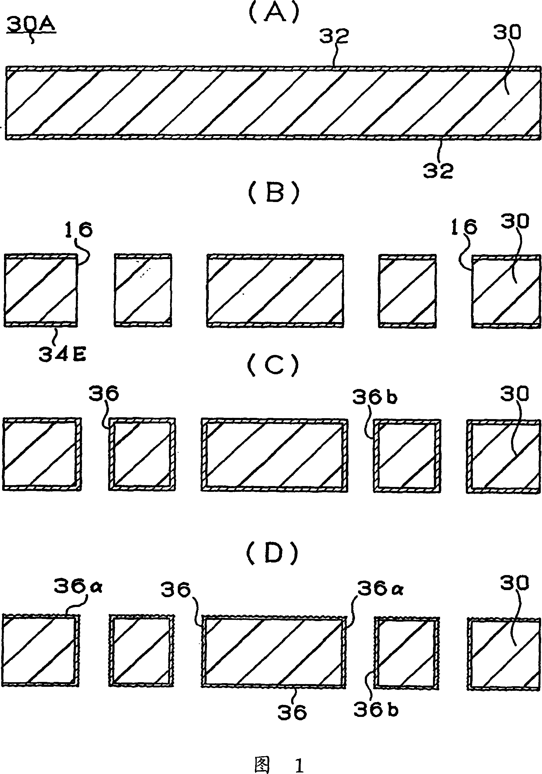
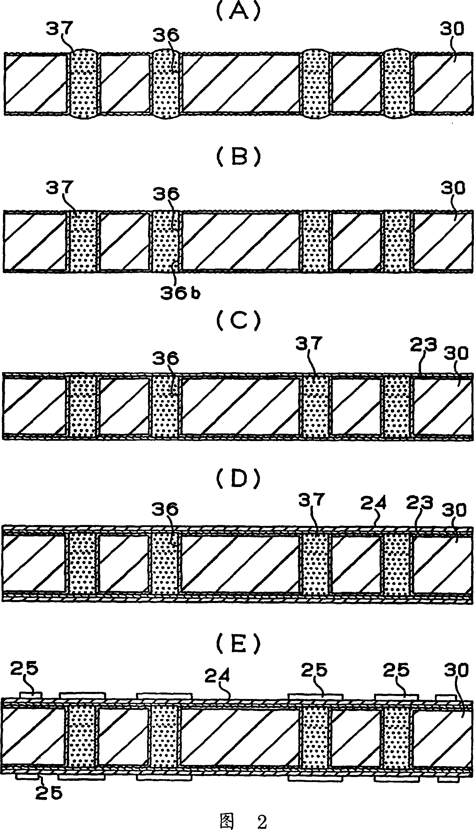
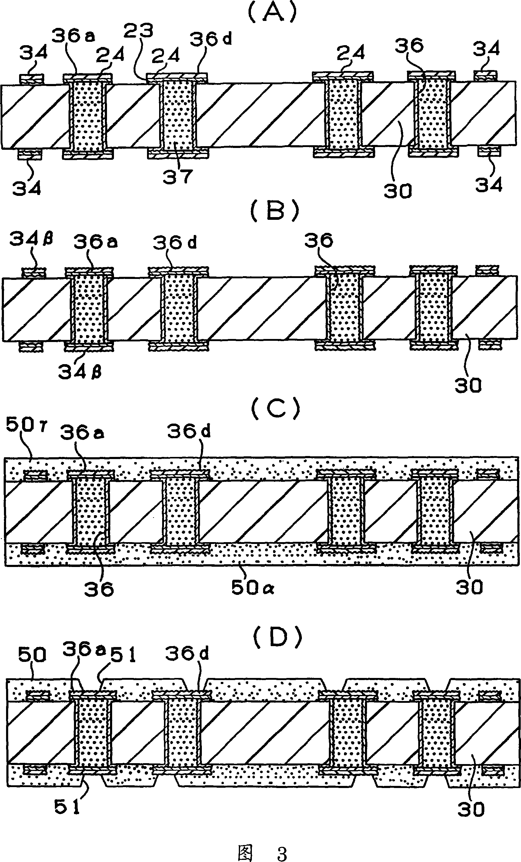
[0029] First, the structure of a multilayer printed wiring board 10 according to a first embodiment of the present invention will be described with reference to FIGS. 1 to 8 . FIG. 7 shows a cross-sectional view of the multilayer printed wiring board 10, and FIG. 8 shows a process of mounting an IC chip 90 on the multilayer printed wiring board 10 shown in FIG. state. As shown in FIG. 7 , in the multilayer printed wiring board 10 , conductor loops 34 are formed on the surface of the core substrate 30 . The front and back surfaces of the core substrate 30 are connected by through holes 36 . The through hole 36 is composed of capping plating layers 36a, 36d constituting the through hole land, and a side wall conductor layer 36b, and the inside of the side wall conductor layer 36b is filled with a resin filling material 37. It is also possible to fill only copper without using a resin filler. The interlaminar resin insulating layer 50 and the interlaminar resin insulating laye...


PUM

PropertyMeasurementUnit
Radiusaaaaaaaaaa
Thicknessaaaaaaaaaa
Thicknessaaaaaaaaaa

Abstract

To provide a multilayer printed wiring board which does not deteriorate connection reliability by using a small diameter via hole. [MEANS FOR SOLVING PROBLEMS] Via holes (60A, 60B) are formed on covering plating layers (36a, 36d) and have via hole bottoms formed within a circle having a radius of R(through hole radius)+r(via hole bottom radius) / 3, with a through hole gravity center at the center. A stress applied on the via holes is smaller than that applied on a via hole (160) formed on a second interlayer resin insulating layer (150). Thus, a bottom diameter of the via holes (60A, 60B) is made smaller than that of the via hole (160).

Description

technical field [0001] The present invention relates to a multilayer printed wiring board, in particular to a laminated multilayer printed wiring board which can be suitably used as a package substrate for IC chip mounting. Background technique [0002] In a build-up multilayer printed wiring board that constitutes a package for an IC chip, an interlayer insulating resin is formed on both sides or one side of a core substrate in which a through hole is formed by a drill, and is opened by laser or photolithography for The via hole for interlayer conduction forms an interlayer resin insulating layer. On the inner wall of the via hole, a conductor layer is formed by plating or the like, and patterned by etching or the like to produce a conductor circuit. Furthermore, by repeating the operation of forming interlayer insulating layers and conductor layers, a build-up multilayer printed wiring board was obtained. In the latest build-up multilayer circuit board, in order to incre...

Claims


Application Information

Patent Timeline
IPC IPC(8): H05K3/46H01R12/51
CPCH05K3/4602H05K2201/09627H05K2201/0959H05K2201/0352H05K2201/0347H05K1/115H05K2201/09509H05K2201/096H05K2201/09454H01L2224/16225H01L2924/15311Y10T29/49165H05K3/42H05K3/46
Inventor 吴有红
Owner IBIDEN CO LTD
Why Eureka
Try Eureka