
Printed wiring board, method for forming the printed wiring board, and board interconnection structure

A technology for printed circuit boards and interconnection structures, which is applied in the structural connection of printed circuits, printed circuits, and printed circuit manufacturing. It can solve the problems of easy peeling and reduced connection strength, and achieve the goal of enhancing connection strength and preventing peeling strength. Reduced effect

Inactive Publication Date: 2007-11-28
THE FUJIKURA CABLE WORKS LTD
View PDF3 Cites 26 Cited by
  • Summary
  • Abstract
  • Description
  • Claims
  • Application Information

AI Technical Summary

Problems solved by technology

Therefore, when a stress that peels the flexible wiring board from the rigid wiring board is applied thereto, peeling easily occurs at the contact surface between the connection terminal and the insulating layer, resulting in a decrease in the overall connection strength.

Method used


Image

  • Printed wiring board, method for forming the printed wiring board, and board interconnection structure
  • Printed wiring board, method for forming the printed wiring board, and board interconnection structure
  • Printed wiring board, method for forming the printed wiring board, and board interconnection structure

Examples


Embodiment Construction

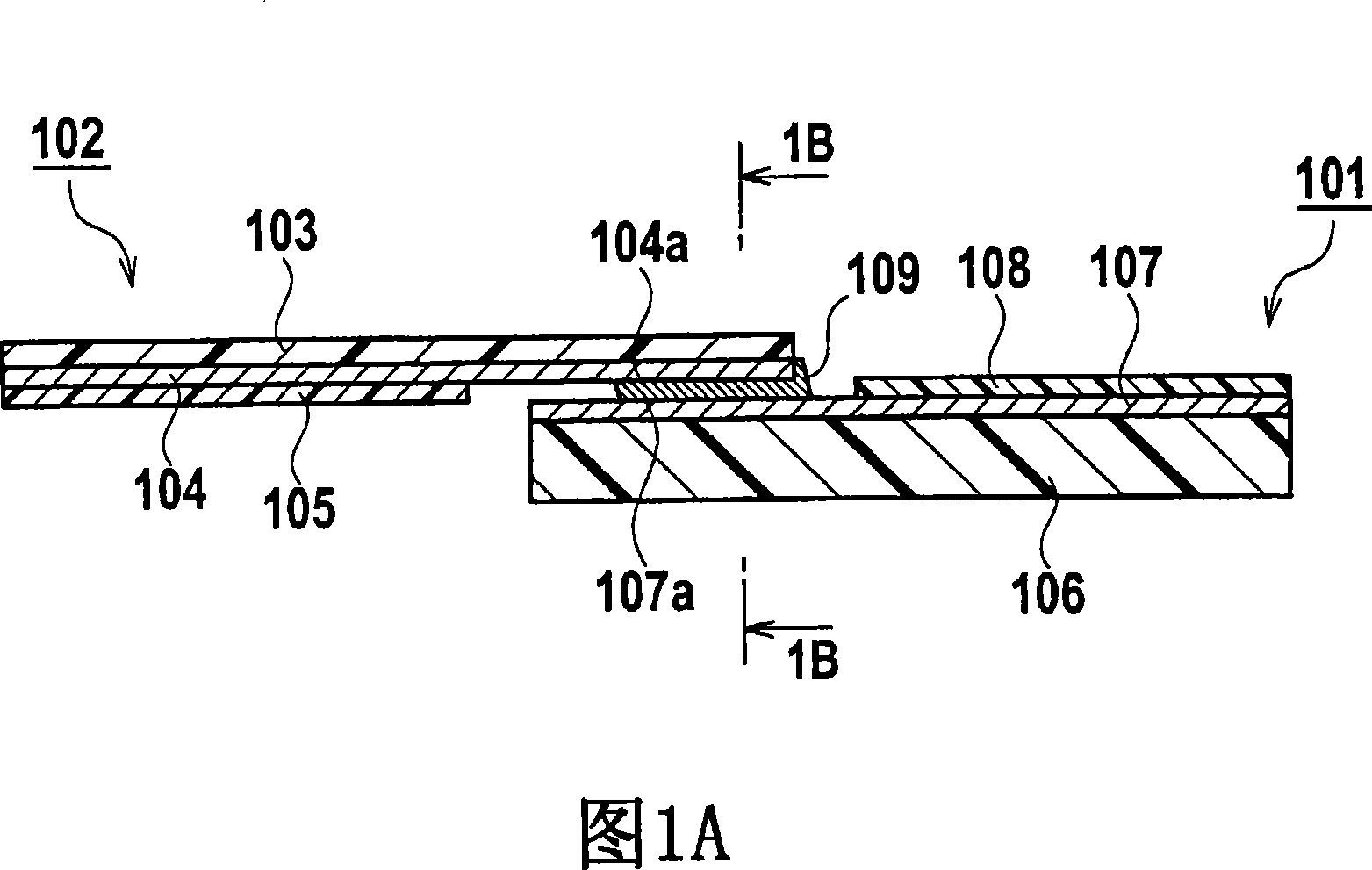
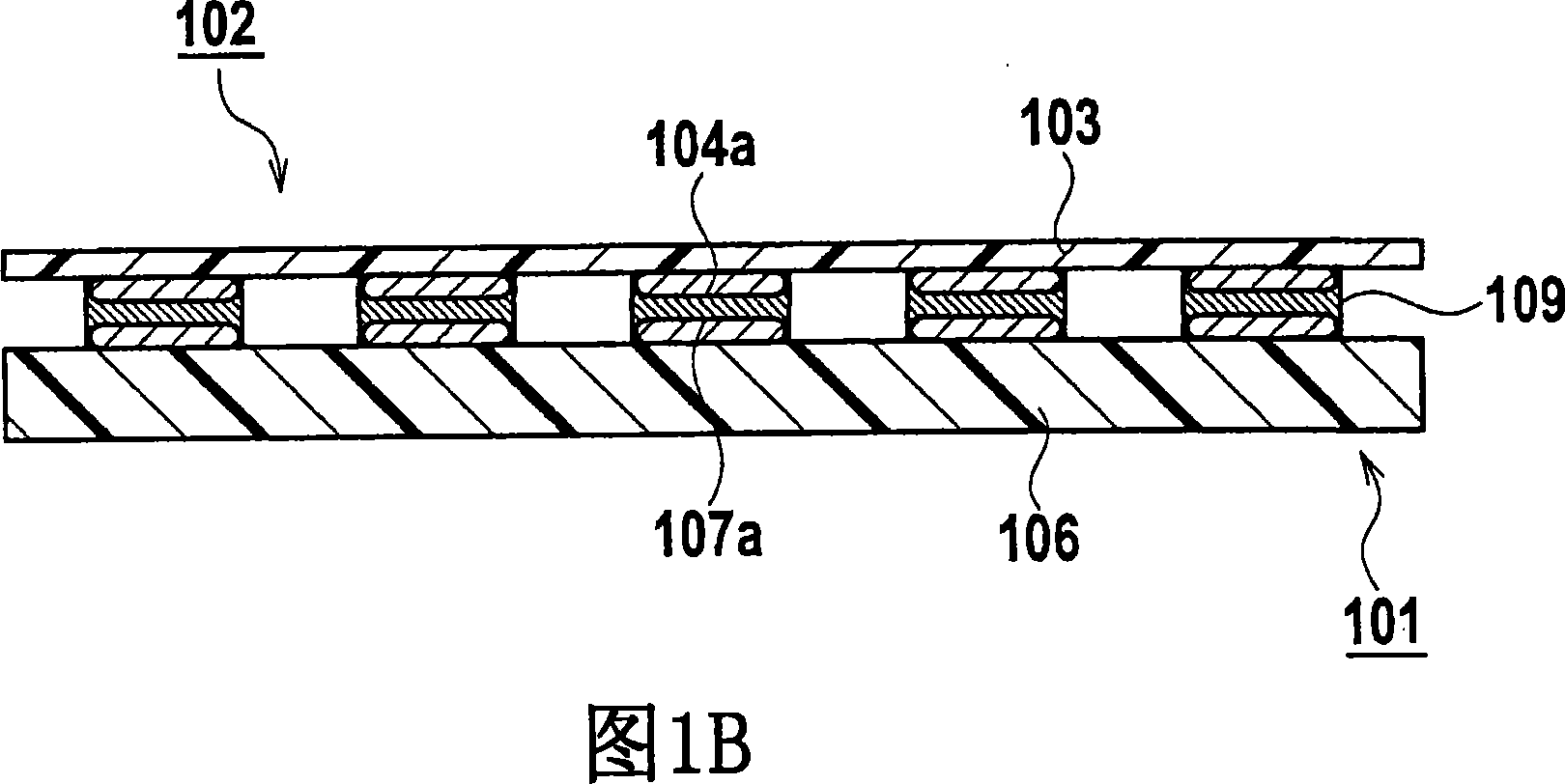
[0034]Non-limiting embodiments of the invention will be described below with reference to the accompanying drawings. In the following description, the same or similar parts of the drawings are identified by the same or similar reference numerals. It is to be noted that the drawings are only schematic, and the relationship between the thickness and planar dimensions, the ratio of the thickness of each layer, and the like are different from the actual ones. Therefore, specific thicknesses and dimensions are determined by referring to the following description. Furthermore, in the drawings, it is inevitable to include portions where the relationship and ratio of dimensions are different from each other.

[0035] (first non-limiting embodiment)

[0036] (printed circuit board)

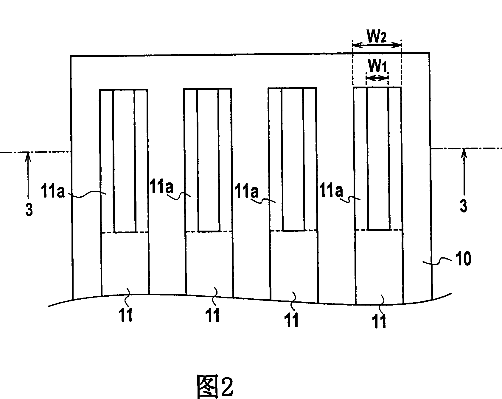
[0037] As shown in FIG. 2, the printed wiring board according to the first embodiment of the present invention includes an insulating layer 10, a conductive circuit 11 having connection terminals 11a on...


PUM


Abstract

A board interconnection structure having a first printed wiring board in which a first conductive circuit is arranged on a first insulating layer, the first conductive circuit having, on an end portion thereof, a first connection terminal in which an upper surface width is narrower than a bottom surface width; a second printed wiring board in which a second conductive layer having a second connection terminal is arranged on a second insulating layer; and a connection layer that forms fillets along longitudinal side surfaces of the first connection terminal, and interconnects the first connection terminal and the second connection terminal. The first connection terminal may have a projection portion.

Description

[0001] This application claims priority from Japanese Patent Applications Nos. 2006-145389 and 2006-145390 filed on May 25, 2006, the entire contents of which are incorporated herein by reference. technical field [0002] This application relates to techniques for interconnecting printed boards. In particular, the present invention relates to a printed wiring board, a method for forming a printed wiring board, and a board interconnection structure capable of enhancing the interconnection strength of the board. Background technique [0003] As electronic equipment is required to be smaller in size, lighter in weight, and more advanced in function, it is more necessary to three-dimensionally install multiple boards in a small space of a product. For this reason, the space for connecting electrical signals between the boards must be reduced. However, if the functions of electronic equipment become more advanced, the types of electrical signals between boards will also increase...

Claims


Application Information

Patent Timeline
Patent Type & Authority Applications(China)
IPC IPC(8): H05K1/14H05K3/02
CPCH01L2924/0002
Inventor 北田智史圆尾弘树高见良
Owner THE FUJIKURA CABLE WORKS LTD
Learn More