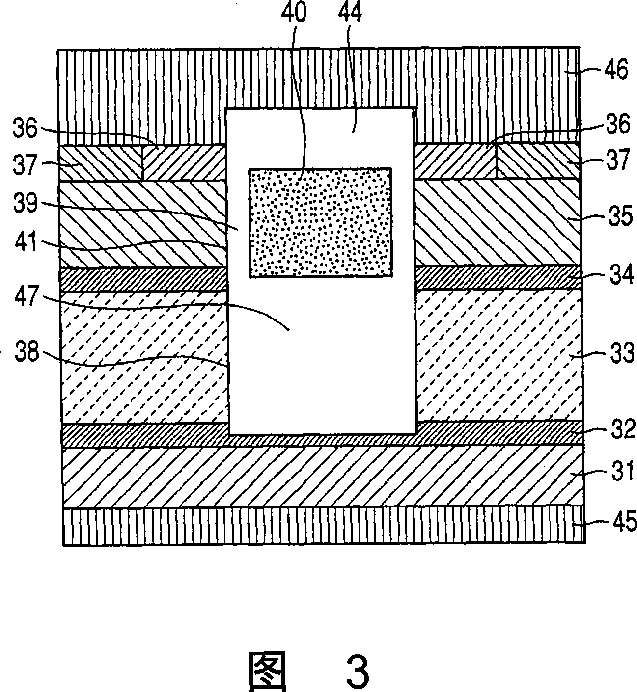
Silicon carbide semiconductor device and manufacturing method thereof
A manufacturing method and semiconductor technology, applied in semiconductor/solid-state device manufacturing, semiconductor devices, electrical components, etc., can solve problems such as difficulty in reducing channel resistance, difficulty in further reducing on-resistance, and improving MOS channel mobility, etc.
- Summary
- Abstract
- Description
- Claims
- Application Information
AI Technical Summary
Problems solved by technology
Method used
Image
Examples
example 1
[0043] In Example 1, a method of manufacturing an n-type SiC-MOS capacitor according to the present invention will be described. The change in conductivity type allows p-type SiC-MOS capacitors to be fabricated in the same manner as in Example 1 explained below. Furthermore, devices such as n-channel or p-channel MOSFETs can be easily manufactured by forming components such as source, drain, and gate electrodes using known methods.
[0044] First, prepare an alumina boat. Upstream from this boat, a SiC pseudo-substrate (not necessarily single crystal) is placed on which 5 mm thick SiO 2 . The width of the dummy substrate sample to the gas flow is taken to be at least wider than the width (50.8 mm in diameter) of the SiC substrate sample to be initially processed described later, eg, a 55 mm square. Downstream from the boat, SiC substrate samples were set up for fabrication of n-type SiC-MOS capacitors according to the present invention.
[0045] In Example 1, for a sample ...
example 2
[0058] In Example 2, a method of manufacturing an n-type SiC-MOS capacitor according to the present invention will also be explained. As in Example 1, modification of the conductivity type of the SiC substrate of course allows the formation of p-type MOS capacitors and n-channel or p-channel MOSFETs. In the following, the differences from Example 1 are especially emphasized for explanation.
[0059] In Example 2, a double tube of quartz glass was used for the heat treatment system. This system has a structure in which cooling water is made to flow between an outer tube and an inner tube of a double tube. According to the present invention with SiO formed thereon 2 SiC substrate samples and dummy samples were mounted on polycrystalline SiC-coated high-purity graphite susceptors. The susceptor is set on a susceptor holder of quartz glass with a thick pad of high-purity porous graphite placed therebetween so that the susceptor is not in direct contact with the double tube of q...
example 3
[0064] In Example 3, a method of manufacturing an n-type capacitor according to the present invention was explained. As in Examples 1 and 2, p-type MOS capacitors and n-channel or p-channel MOSFETs can be formed. In Example 3, the differences from Examples 1 and 2 are especially emphasized.
[0065] The heat treatment system used in Example 3 is a system in which a hollow heat insulator of high-purity graphite is placed in a reaction tube of quartz glass of a SiC epitaxial growth system and a high-purity graphite susceptor coated with polycrystalline SiC is disposed inside the heat insulator, as SiO for use according to the present invention 2 The heat treatment system is provided. The graphite susceptor is grooved horizontally. Along this groove, a polycrystalline SiC substrate is placed. On the polycrystalline SiC substrate, a SiC substrate sample and a dummy substrate according to the present invention were mounted (the dummy substrate was mounted upstream). The graphi...
PUM
| Property | Measurement | Unit |
|---|---|---|
| thickness | aaaaa | aaaaa |
| melting point | aaaaa | aaaaa |
| melting point | aaaaa | aaaaa |
Abstract
Description
Claims
Application Information
 - R&D Engineer
- R&D Manager
- IP Professional
- Industry Leading Data Capabilities
- Powerful AI technology
- Patent DNA Extraction
Browse by: Latest US Patents, China's latest patents, Technical Efficacy Thesaurus, Application Domain, Technology Topic, Popular Technical Reports.
© 2024 PatSnap. All rights reserved.Legal|Privacy policy|Modern Slavery Act Transparency Statement|Sitemap|About US| Contact US: help@patsnap.com


