Structure of peltier element or seebeck element and its manufacturing method
A manufacturing method and Seebeck coefficient technology, which are applied in the manufacture/processing of thermoelectric devices, junction lead-out materials of thermoelectric devices, thermoelectric devices using only Peltier or Seebeck effect, etc. Reduced utilization efficiency and other issues
- Summary
- Abstract
- Description
- Claims
- Application Information
AI Technical Summary
Problems solved by technology
Method used
Image
Examples
Embodiment Construction
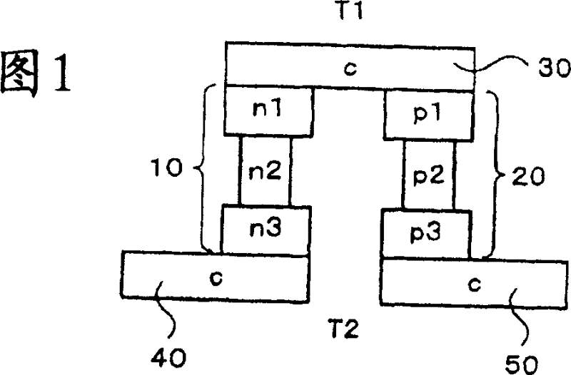
[0066] Hereinafter, the structure and manufacturing method of the Peltier element or Seebeck element of the present invention will be described with reference to the drawings. FIG. 1 is a schematic configuration diagram of a Peltier element or a Seebeck element according to a first embodiment of the present invention.
[0067] As shown in FIG. 1 , a first conductive member (n-type semiconductor, etc.) 10 having a predetermined Seebeck coefficient includes two end portions n1 and n3 and a middle portion n2. In addition, the second conductive member (p-type semiconductor, etc.) 20 having a Seebeck coefficient different from that of the first conductive member includes two end portions p1 and p2 and an intermediate portion p2.
[0068] The middle portions n2 and p2 of the first conductive member 10 and the second conductive member 20 have a cross section smaller than that of the two end portions n1, n3, p1, p3. Therefore, the thermal conductivity of the middle portion becomes sm...
PUM
 Abstract
Description
Claims
Application Information
 - R&D
- Intellectual Property
- Life Sciences
- Materials
- Tech Scout
- Unparalleled Data Quality
- Higher Quality Content
- 60% Fewer Hallucinations
Browse by: Latest US Patents, China's latest patents, Technical Efficacy Thesaurus, Application Domain, Technology Topic, Popular Technical Reports.
© 2025 PatSnap. All rights reserved.Legal|Privacy policy|Modern Slavery Act Transparency Statement|Sitemap|About US| Contact US: help@patsnap.com


