Slow wave structure based on electromagnetic band gap structure
A technology of electromagnetic band gap structure and slow wave structure, applied in the field of physical electronics, can solve problems such as difficult to satisfy the structure, and achieve the effects of increased operating bandwidth, good heat dissipation characteristics, and efficient energy exchange
- Summary
- Abstract
- Description
- Claims
- Application Information
AI Technical Summary
Problems solved by technology
Method used
Image
Examples
Embodiment 1
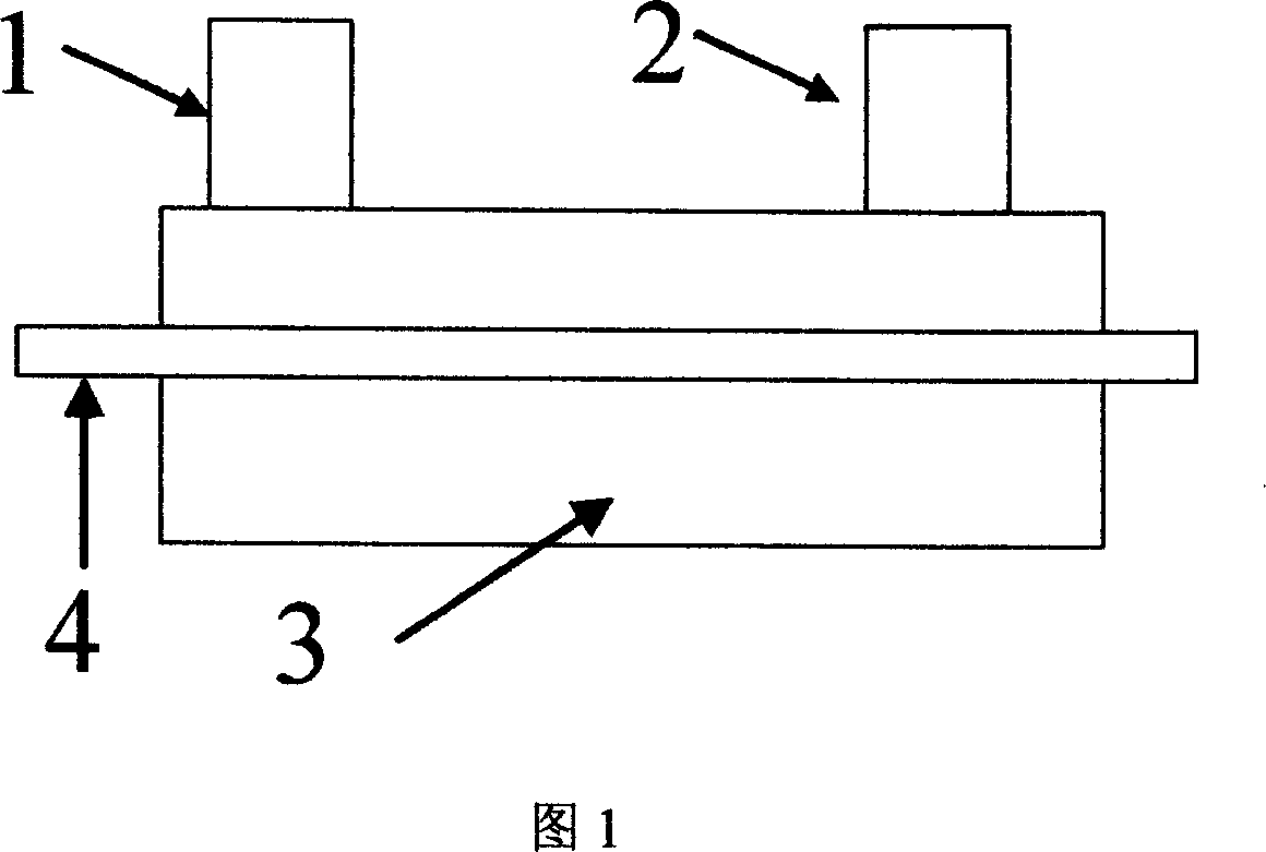
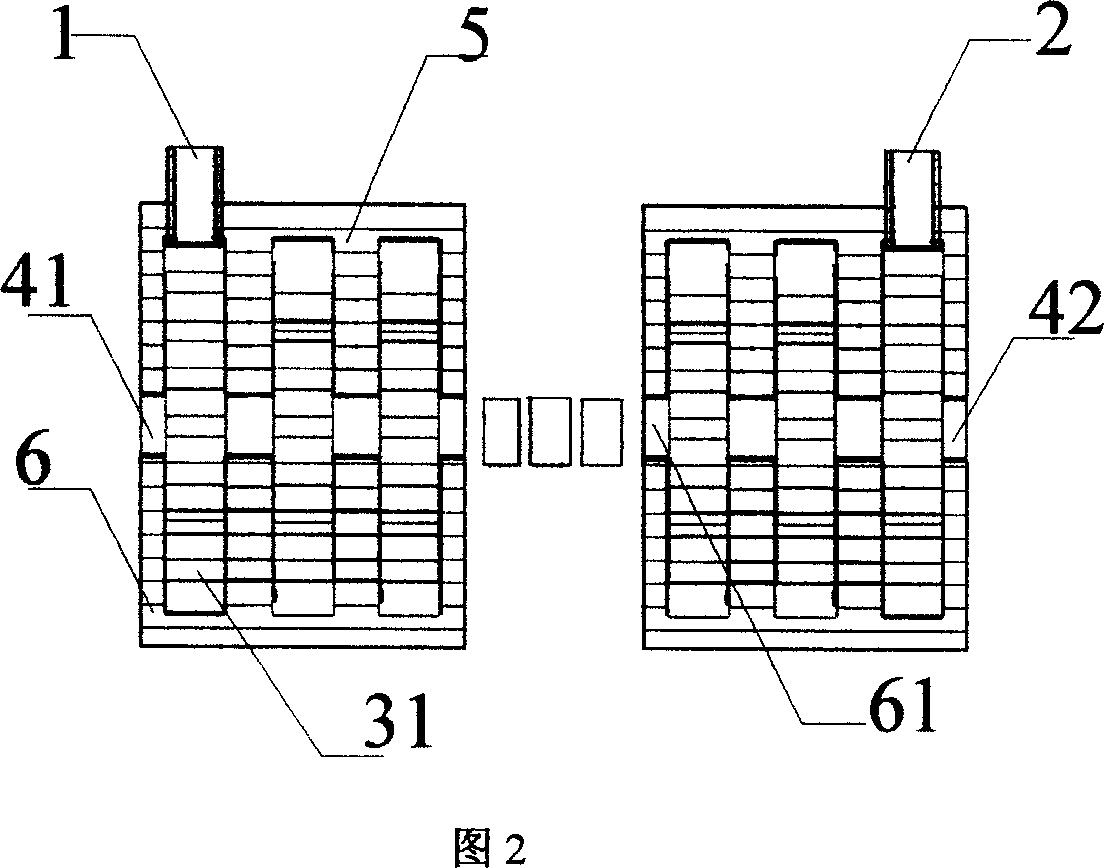
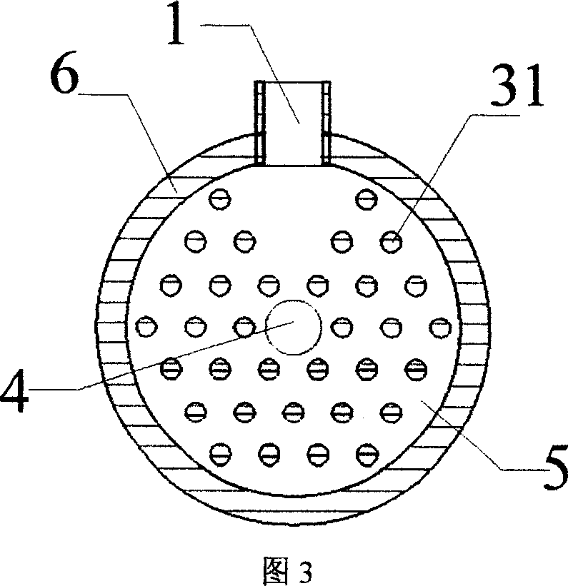
[0020] Embodiment 1: With reference to Fig. 1, Fig. 2 and Fig. 3, a kind of slow wave structure based on electromagnetic bandgap structure, comprises electromagnetic bandgap structure 3, is provided with input channel 1, output channel 2 and electronic channel 1 on the electromagnetic bandgap structure The injection channel 4, the electron injection channel 4 runs through the electromagnetic bandgap structure, the electromagnetic bandgap structure includes a cavity 5, a metal separator 6 and a metal rod 31 are arranged in the cavity 5, and an electron injection channel 4 is arranged on the cavity 5 The electron injection port 41 and the electron injection port 42 are provided with a window 61 which doubles as an electromagnetic wave channel and an electron injection channel on the metal separator 6 .
[0021] In this embodiment, the blocks between the structures in FIG. 2 indicate that the electromagnetic bandgap structure can adopt any period in this direction. The electromag...
Embodiment 2
[0022] Embodiment 2: With reference to Fig. 1, Fig. 5 and Fig. 6, a kind of slow wave structure based on electromagnetic bandgap structure, comprises electromagnetic bandgap structure 3, is provided with input channel 1, output channel 2 and electron The injection channel 4, the electron injection channel 4 runs through the electromagnetic bandgap structure, the electromagnetic bandgap structure includes a cavity 5, a metal partition 6 and a metal rod 31 are arranged in the cavity 5, and an electromagnetic wave window 62 is arranged on the metal partition 6 And the electromagnetic wave windows 62 on the two adjacent metal partitions 6 are located on both sides of the cavity 5 respectively, and the electron injection channel 4 is composed of the electron injection port 41, the electron injection port 42 located on the cavity 5, and the electron injection port 42 located on the metal partition 6. The electron injection window 61 on the top constitutes.
[0023] Referring to Figu...
PUM
 Abstract
Description
Claims
Application Information
 - R&D
- Intellectual Property
- Life Sciences
- Materials
- Tech Scout
- Unparalleled Data Quality
- Higher Quality Content
- 60% Fewer Hallucinations
Browse by: Latest US Patents, China's latest patents, Technical Efficacy Thesaurus, Application Domain, Technology Topic, Popular Technical Reports.
© 2025 PatSnap. All rights reserved.Legal|Privacy policy|Modern Slavery Act Transparency Statement|Sitemap|About US| Contact US: help@patsnap.com


