Module with chip connection contact, its data carrier and lead frame structure
A technology for connecting contacts and data carriers, applied to record carriers used in machines, electric solid-state devices, semiconductor devices, etc.
- Summary
- Abstract
- Description
- Claims
- Application Information
AI Technical Summary
Problems solved by technology
Method used
Image
Examples
Embodiment Construction
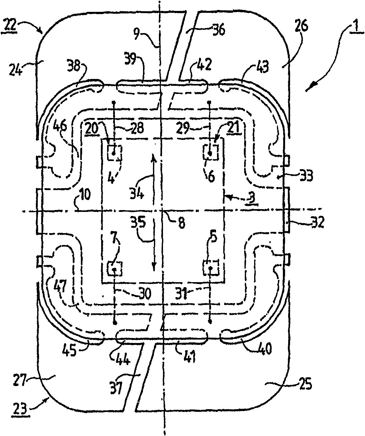
[0026] figure 1 Module 1 is shown. The module 1 is designed in the form of a plate and has as low an overall height as possible: in this case approximately 220 μm. The overall height may range between 190 μm and 400 μm. The module 1 includes a leadframe structure 2 and a chip 3 . The chip 3 includes a circuit (not shown), with the aid of the circuit, it can perform contactless communication with a communication base station suitable for the circuit. Chip 3 has chip connection contacts 4 , 5 and 6 , 7 . We will explore the purpose of connecting contacts 4 to 7 in further detail below.
[0027] The module 1 and the leadframe structure 2 have a midpoint 8 and a main axis 9 passing through the midpoint 8 and a secondary axis 10 likewise passing through the midpoint 8 .
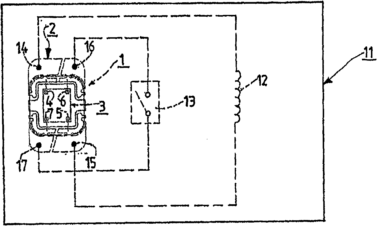
[0028] The module 1 is intended for use in a data carrier 11 designed for contactless communication. exist figure 2 A data carrier 11 is shown in . As an electronic component, the data carrier 11 contains...
PUM
 Abstract
Description
Claims
Application Information
 - R&D
- Intellectual Property
- Life Sciences
- Materials
- Tech Scout
- Unparalleled Data Quality
- Higher Quality Content
- 60% Fewer Hallucinations
Browse by: Latest US Patents, China's latest patents, Technical Efficacy Thesaurus, Application Domain, Technology Topic, Popular Technical Reports.
© 2025 PatSnap. All rights reserved.Legal|Privacy policy|Modern Slavery Act Transparency Statement|Sitemap|About US| Contact US: help@patsnap.com


