Pixel structure of active part array substrates

An array substrate and pixel structure technology, applied in electrical components, electrical solid-state devices, semiconductor devices, etc., can solve the problems of complex process and low yield rate, and achieve the effect of increasing the viewing angle

Active Publication Date: 2009-12-23
AU OPTRONICS CORP
View PDF6 Cites 0 Cited by
  • Summary
  • Abstract
  • Description
  • Claims
  • Application Information

AI Technical Summary

Problems solved by technology

[0006] The purpose of the present invention is to provide a color filter substrate, an active element array substrate and a pixel structure of a liquid crystal display panel, all of which have the characteristics of wide viewing angles, and improve the problems of complex process and low yield

Method used


Image

  • Pixel structure of active part array substrates
  • Pixel structure of active part array substrates
  • Pixel structure of active part array substrates

Examples


Embodiment Construction

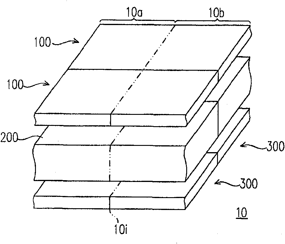
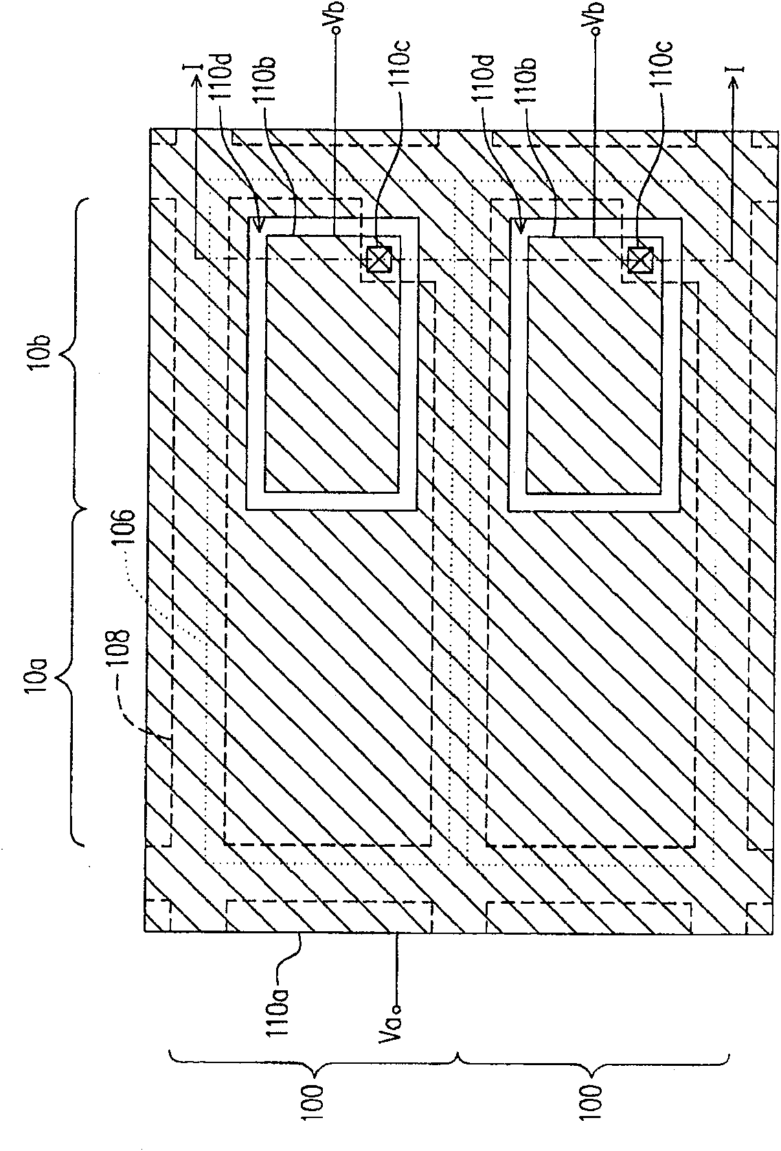
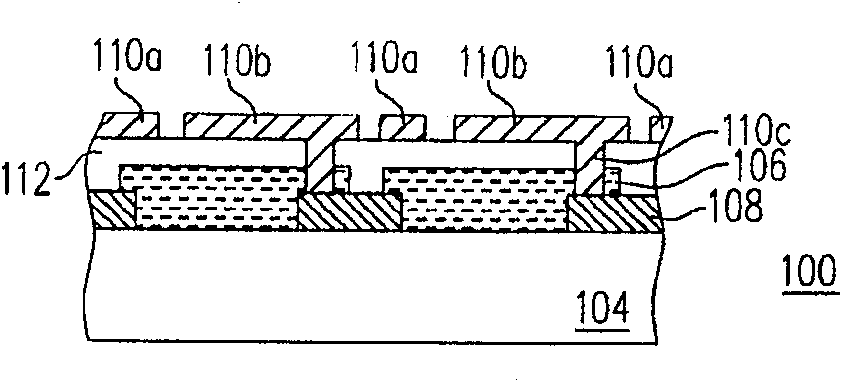
[0067] In order to make the liquid crystal display have the characteristic of wide viewing angle, the present invention divides the color filter substrate, the active element array substrate and the pixel structure of the liquid crystal display panel into two regions. In terms of the pixel structure of the color filter substrate, the common electrodes of the two regions are electrically connected to different voltage input terminals. In terms of the pixel structure of the active device array substrate, the two regions have different pixel electrode areas, gate-drain capacitances or storage capacitances. Therefore, one pixel structure can make the liquid crystal molecules have two kinds of inclination angles, thereby increasing the viewing angle of the liquid crystal display. In addition, the pixel structure of the liquid crystal display panel of the present invention can combine the above configurations to achieve the purpose of increasing the viewing angle. In more detail, t...


PUM


Abstract

The present invention proposes a pixel structure of an active element array substrate, including: a scanning line and a data line arranged on the substrate; a double-drain thin film transistor including a gate, a source, a first drain, and a second drain, The gate is electrically connected to the scanning line, the source is electrically connected to the data line, there is a first gate-drain capacitance between the gate and the first drain, and there is a second gate between the gate and the second drain Drain capacitance; the first pixel electrode and the second pixel electrode are electrically connected to the first drain and the second drain respectively; and the first common wiring and the second common wiring are respectively arranged on the first and second Below the pixel electrode, there is a first storage capacitor between the first common wiring and the first pixel electrode, a second storage capacitor between the second common wiring and the second pixel electrode, and the first and second gate drains The capacitors are different, and the first and second storage capacitors are different. The liquid crystal display of the invention can have better yield and lower manufacturing cost.

Description

[0001] This application is a divisional application of a Chinese invention patent application with an application date of December 4, 2006, an application number of 200610163760.X, and an invention title of "color filter and active element array substrate and pixel structure of a liquid crystal display panel" . technical field [0002] The invention relates to a structure of a liquid crystal display, and in particular to a pixel structure of a color filter substrate, a pixel structure of an active element array substrate and a pixel structure of a liquid crystal display panel. Background technique [0003] The rapid progress of the multimedia society is mostly due to the rapid progress of semiconductor components or man-machine display devices. As far as the display is concerned, the cathode ray tube (Cathode Ray Tube, CRT) has been monopolizing the display market in recent years because of its excellent display quality and economy. However, cathode ray tubes still have man...

Claims


Application Information

Patent Timeline
Patent Type & Authority Patents(China)
IPC IPC(8): H01L27/12H01L23/522G02F1/1362
Inventor 吕安序
Owner AU OPTRONICS CORP
Why Eureka
Try Eureka