Organic EL element and manufacturing method
A manufacturing method and element technology, applied in the field of organic EL elements and their manufacturing, can solve the problems of poor conduction of the upper electrode, breakage of the second electrode, breakage of the light-emitting layer, etc., so as to suppress the degradation of quality, prevent poor conduction, prevent The effect of process damage
- Summary
- Abstract
- Description
- Claims
- Application Information
AI Technical Summary
Problems solved by technology
Method used
Image
Examples
no. 1 approach
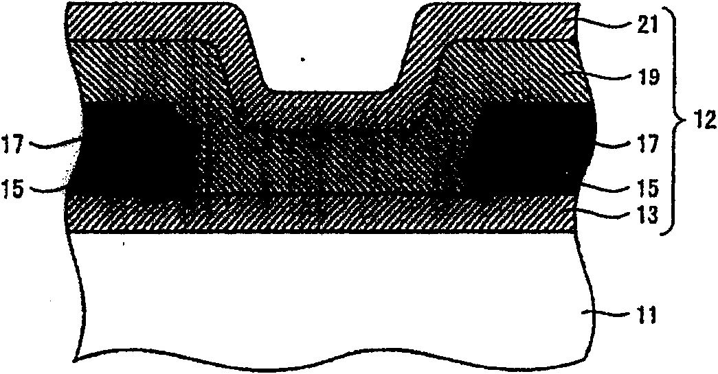
[0045] figure 1 It is a cross-sectional view showing a schematic structure of the organic EL element according to the first embodiment of the present invention. Such as figure 1 As shown, the organic EL element of the present embodiment is constituted to include: a base portion 11 on which driving elements such as TFTs and wiring for driving the organic EL element are formed on a base such as a glass substrate; The light emitting element portion 12 is formed with an organic EL element. Furthermore, the organic EL element of the present embodiment adopts a top emission type (top emission) structure in which light is taken in from the upper surface side (the side of the organic electroluminescent element portion 12 ). In addition, although the planarization layer for planarizing the upper layer such as the above-mentioned TFTs and wirings is provided on the base part 11, since it is not directly related to the gist of the present invention, detailed description and illustratio...
no. 2 approach
[0083] Figure 10 It is a cross-sectional view showing the structure of the organic EL element according to the second embodiment of the present invention. Here, the description will mainly be given to structures different from those of the organic EL element of the first embodiment, and the description of other common structures will be omitted in principle.
[0084] In this embodiment, unlike the first embodiment, the protective material layer 15a in the opening of the interlayer insulating layer 17 is not completely removed, but a part of the protective material layer 15a in the opening of the interlayer insulating layer 17 remains. , thereby forming the recessed portion 15 b in the protective layer 15 . As a result, the film thickness of protective layer 15 in the inner region of the opening of interlayer insulating layer 17 is set smaller than the film thickness of protective layer 15 in the outer region of the opening of interlayer insulating layer 17 .
[0085] By ado...
PUM
 Abstract
Description
Claims
Application Information
 - R&D
- Intellectual Property
- Life Sciences
- Materials
- Tech Scout
- Unparalleled Data Quality
- Higher Quality Content
- 60% Fewer Hallucinations
Browse by: Latest US Patents, China's latest patents, Technical Efficacy Thesaurus, Application Domain, Technology Topic, Popular Technical Reports.
© 2025 PatSnap. All rights reserved.Legal|Privacy policy|Modern Slavery Act Transparency Statement|Sitemap|About US| Contact US: help@patsnap.com


