Field emitting display of electronic emitting source including forming multilayer structure

An electron emission source and electron emission technology, applied in the direction of image/graphic display tube, discharge tube/lamp manufacturing, discharge tube/lamp parts, etc., can solve the problems of shortened life of electron emission source, high energy consumption, etc.

Inactive Publication Date: 2009-05-13
SAMSUNG SDI CO LTD
View PDF5 Cites 0 Cited by
  • Summary
  • Abstract
  • Description
  • Claims
  • Application Information

AI Technical Summary

Problems solved by technology

In addition to consuming more energy, the application of high voltage results in a shortened lifetime of the electron emission source

Method used


Image

  • Field emitting display of electronic emitting source including forming multilayer structure
  • Field emitting display of electronic emitting source including forming multilayer structure
  • Field emitting display of electronic emitting source including forming multilayer structure

Examples


Embodiment Construction

[0030] Preferred embodiments of the present invention will now be described in detail with reference to the accompanying drawings.

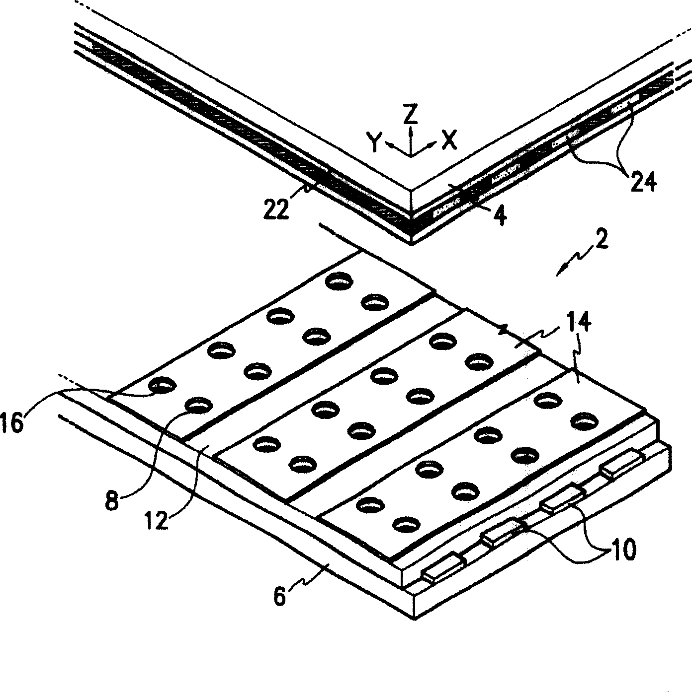
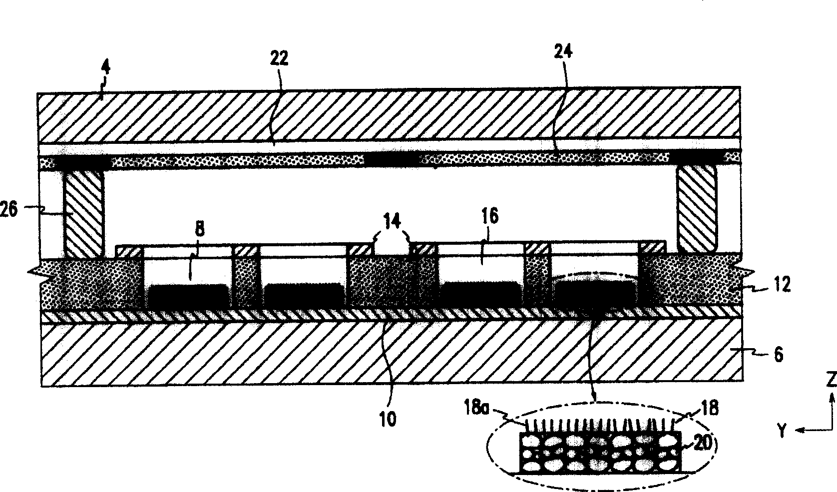
[0031] figure 1 is a partial perspective view of a field emission display according to a first preferred embodiment of the present invention, figure 2 is a partial sectional view of the field emission display according to the first preferred embodiment of the present invention.

[0032] A field emission display (FED) 2 includes a front substrate 4 and a rear substrate 6 disposed opposite to each other at a predetermined interval to form a vacuum device. An electron emission source 8 and a structure for generating an electric field required for electron emission are disposed on the rear substrate 6 , while a structure capable of realizing a predetermined image by emitting visible light using electrons is disposed on the front substrate 4 .

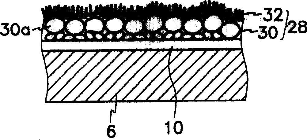
[0033] More specifically, cathode electrodes 10 are formed in a stripe pattern on the rear substrate 6 ...


PUM


Abstract

A field emission display includes first and second substrates provided opposing one another with a predetermined gap therebetween; electron emission sources provided on one of the first and second substrates; an electron emission inducing assembly for inducing the emission of electrons from the electron emission sources; and an illuminating assembly provided on the substrate on which the electron emission sources are not formed, the illuminating assembly realizing images by the emission of electrons from the electron emission sources. The electron emission sources include a carbon nanotube layer and a base layer, the base layer connecting the carbon nanotube layer to the substrate and applying a voltage to the carbon nanotube layer required for the emission of electrons. Also, the carbon nanotube layer is provided on the base layer in a state substantially un-mixed with the base layer.

Description

technical field [0001] The present invention relates to field emission displays, and more particularly, to field emission displays including electron emission sources using carbon nanotubes. Background technique [0002] The first field emission displays used Spindt-type electron emission sources in which a material such as molybdenum or silicon was layered and sharp points were formed in multiple locations. However, the Spindt-type electron emission source complicates processing due to its fine structure, and requires high-precision processing. These factors make it difficult to apply the Spindt-type electron emission source to a display device having a large screen size. [0003] Accordingly, efforts are being made to simplify processing and facilitate production of display devices having a large screen size by forming flat electron emission sources using carbon-based materials. [0004] Carbon-based materials suitable for forming electron emission sources include graphi...

Claims


Application Information

Patent Timeline
Patent Type & Authority Patents(China)
IPC IPC(8): H01J31/12H01J29/04H01J29/46H01J1/304H01J1/30H01J9/02
CPCH01J1/3048H01J2201/30469H01J31/127B82Y10/00H01J9/025C01B32/05H01J1/30
Inventor 柳美爱金薰英南仲佑
Owner SAMSUNG SDI CO LTD
Why Eureka
Try Eureka