CrN/CrAlN protective coating capable of resisting high temperature corrosion in wide temperature range and preparing method
A protective coating and wide temperature technology, applied in the coating, metal material coating process, ion implantation plating, etc., to achieve the effect of simple structure, protection against low-temperature oxidation and thermal corrosion, and excellent high-temperature protection performance
- Summary
- Abstract
- Description
- Claims
- Application Information
AI Technical Summary
Problems solved by technology
Method used
Image
Examples
Embodiment 1
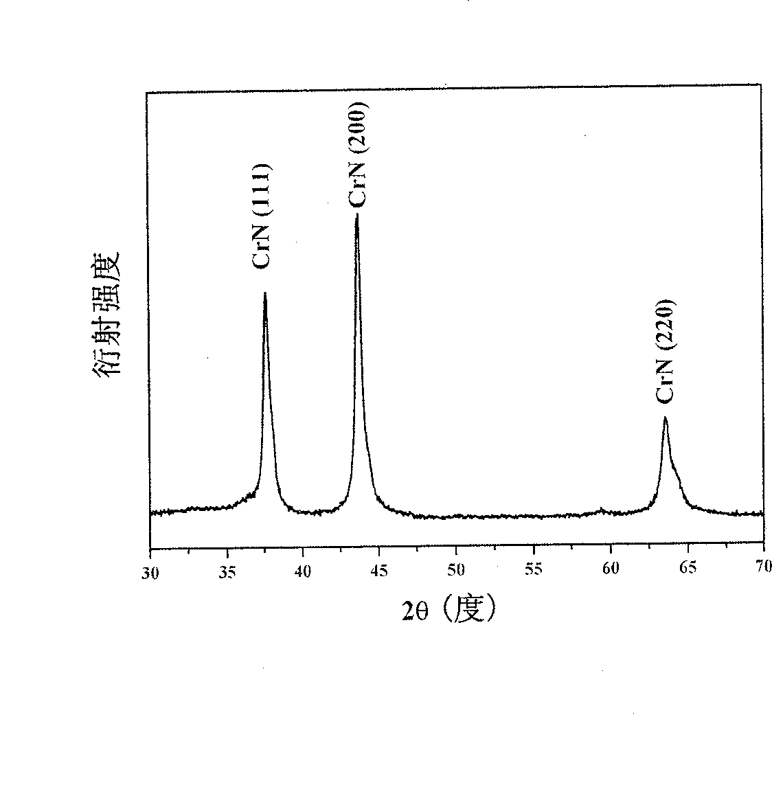
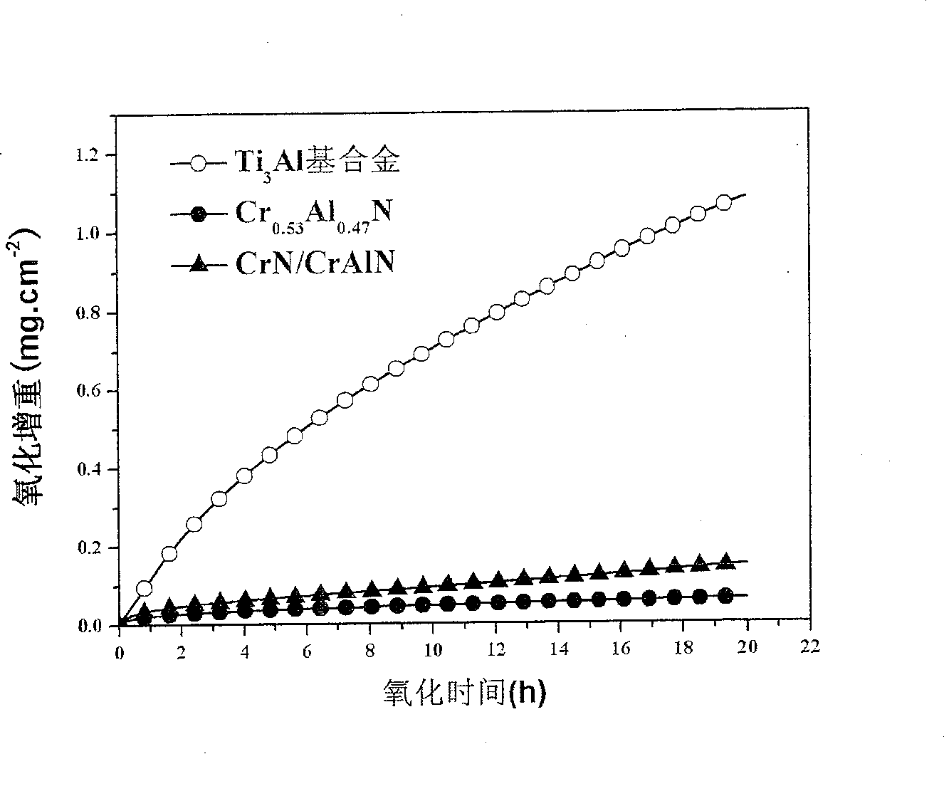
[0021] The surface will be pre-treated by sandblasting, and the size will be 10×20×2mm 3 Ti 3 Put the Al-based alloy substrate into the vacuum coating equipment, and evacuate until the background vacuum degree is 4×10 -4 After Pa, the substrate is heated to 300°C. Open the intake valve to fill in 12SCCM of nitrogen and 8SCCM of argon, adjust the vacuum degree to 0.5Pa by adjusting the opening and closing of the gate valve, and then turn on the DC power connected to the Cr target, at a power density of 4.2W / cm 2 A single layer of CrN layer was sputtered for 5 hours, and the thickness of the CrN layer was 8 μm. Then turn on the DC power connected to the Al target, and co-sputter the Cr-Al-N layer with the Cr target, and the thickness of the Cr-Al-N layer is 8 μm. During the sputtering process, the power density of the Cr target and the Al target appears in the following four pairs: 4.2 / 4.2, 3.0 / 4.2, 2.1 / 4.2, 1.5 / 4.2. And the sputtering time of each power density pairing form...
Embodiment 2
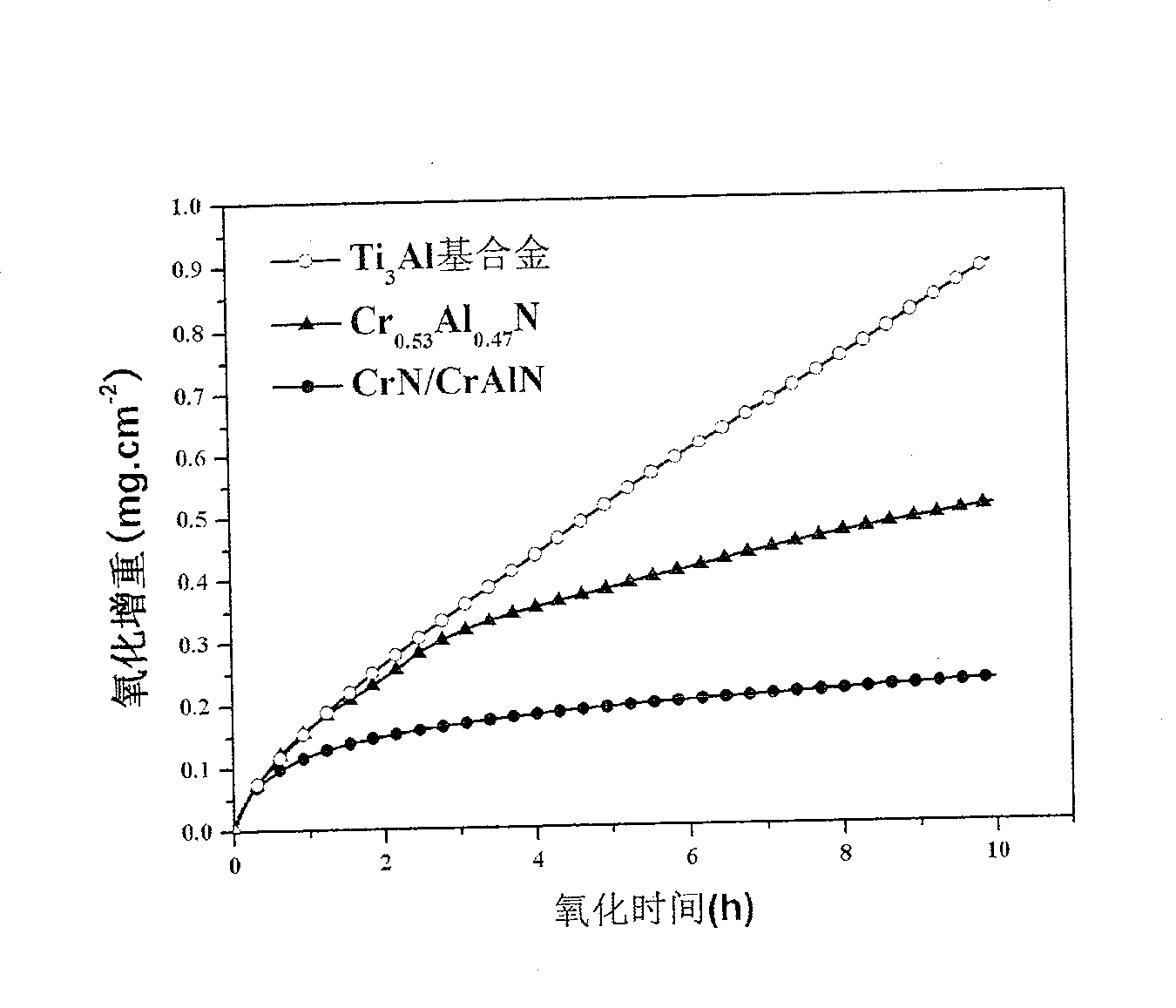
[0023] Will be surface pre-treated, size 10×20×2mm 3 Put the K38G alloy substrate into the vacuum coating equipment, and evacuate until the background vacuum degree is 4×10 -4 After Pa, the substrate is heated to 250°C. Open the intake valve to fill in 8 SCCM of nitrogen and 12 SCCM of argon, adjust the vacuum degree to 0.2Pa by adjusting the opening and closing of the gate valve, and then turn on the DC power supply connected to the Cr target, at a power density of 2.1W / cm 2A single layer of CrN layer was sputtered for 10 hours, and the thickness of the CrN layer was 16 μm. Then turn on the DC power connected to the Al target, and co-sputter the Cr-Al-N layer with the Cr target, and the thickness of the Cr-Al-N layer is 10 μm. During the sputtering process, the power density of the Cr target and the Al target appears in the following four pairs: 4.2 / 4.2, 3.0 / 4.2, 2.1 / 4.2, 1.5 / 4.2. And the sputtering time of each power density pairing form is 1h, 3h, 5h, 7h respectively. ...
PUM
| Property | Measurement | Unit |
|---|---|---|
| thickness | aaaaa | aaaaa |
| thickness | aaaaa | aaaaa |
Abstract
Description
Claims
Application Information
 - R&D
- Intellectual Property
- Life Sciences
- Materials
- Tech Scout
- Unparalleled Data Quality
- Higher Quality Content
- 60% Fewer Hallucinations
Browse by: Latest US Patents, China's latest patents, Technical Efficacy Thesaurus, Application Domain, Technology Topic, Popular Technical Reports.
© 2025 PatSnap. All rights reserved.Legal|Privacy policy|Modern Slavery Act Transparency Statement|Sitemap|About US| Contact US: help@patsnap.com


