Optical sensory element and its manufacturing method

A light sensor, conductive type technology, applied in the field of clip-on photodiode structure, can solve the problem of not covering shallow trench insulation structure, incompatibility, difficult to control shallow source/drain junction of clip-on photodiode, etc. problem, to achieve the effect of improving dark current characteristics and response improvement

Active Publication Date: 2008-10-22
TAIWAN SEMICON MFG CO LTD
View PDF2 Cites 0 Cited by
  • Summary
  • Abstract
  • Description
  • Claims
  • Application Information

AI Technical Summary

Problems solved by technology

[0004] However, the clip-on photodiode is not compatible with the traditional STI technology because it is difficult to control the formation of the shallow source / drain junction and cannot cover the corners of the STI structure in the traditional process. )

Method used


Image

  • Optical sensory element and its manufacturing method
  • Optical sensory element and its manufacturing method
  • Optical sensory element and its manufacturing method

Examples


Embodiment Construction

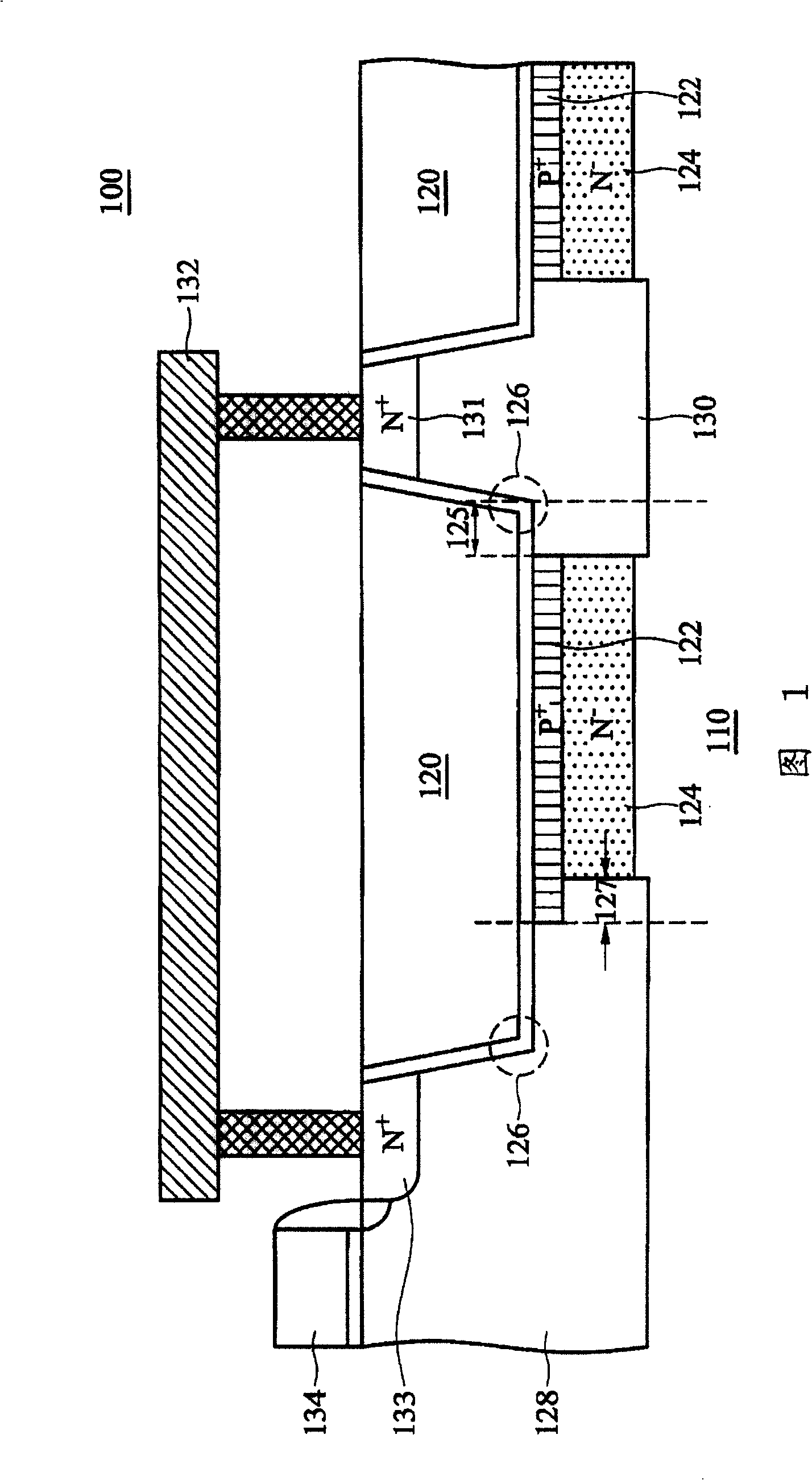
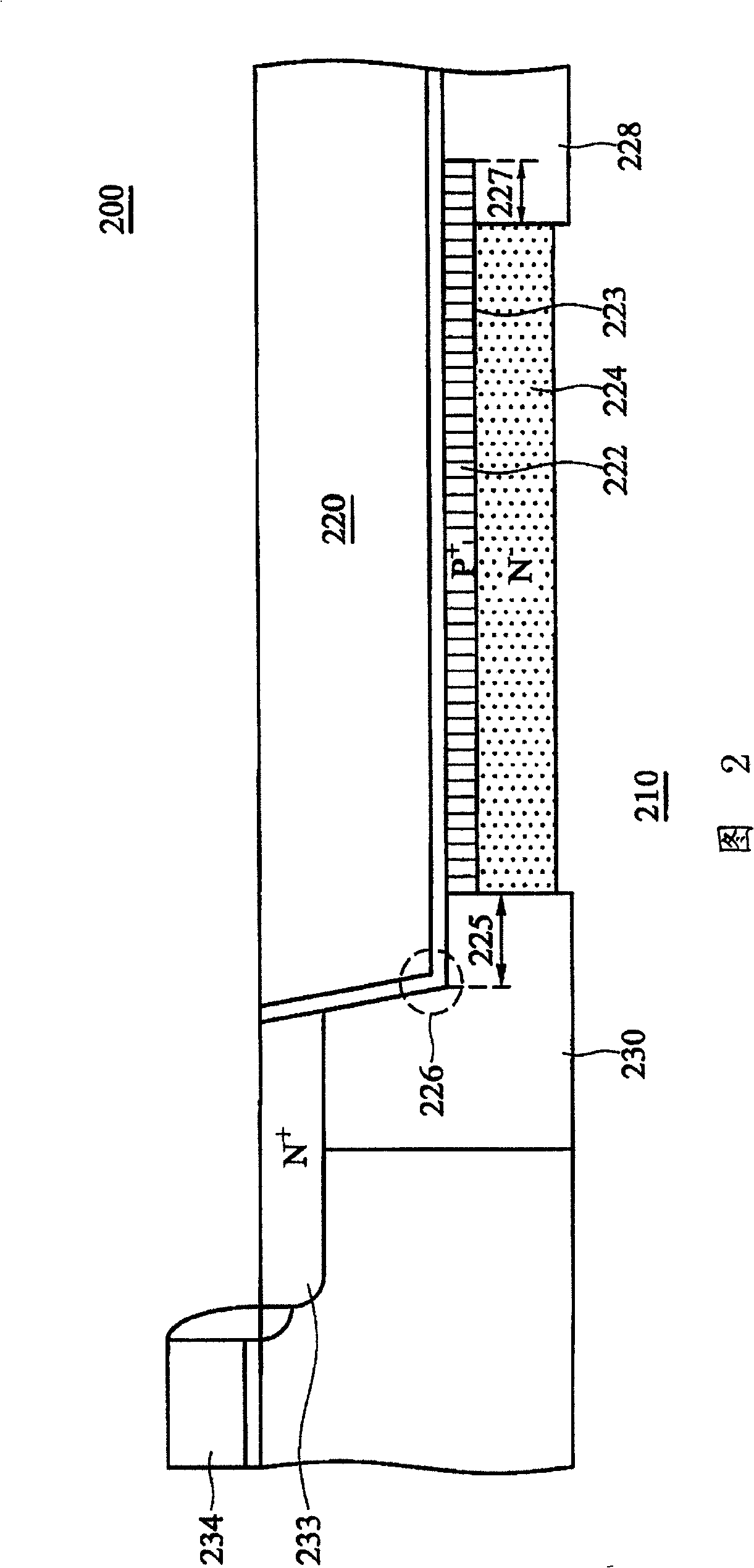
[0026] The structure of the light sensor according to the embodiments of the present invention will be described below. Although the disclosed embodiments are NPN-type clip-on photodiode structures, these embodiments are also applicable to PNP-type clip-on photodiodes. structure.

[0027] FIG. 1 illustrates a photosensor according to an embodiment of the present invention. The photosensor 100 includes a P-type substrate 110, at least one trench 120 formed in the substrate, and at least one P-type heavily doped region. 122 and at least one N-type lightly doped region 124, each P-type heavily doped region 122 is formed under a corresponding trench 120, each N-type lightly doped region is located in the corresponding P-type doped region 122 Between the substrate 110, the P-type heavily doped region 122 or the N-type lightly doped region 124 will not extend beyond the corner 126 of the trench. The distance 125 is between 0.1 and 0.3 microns; since there will still be some disloca...


PUM


Abstract

The invention provides a photo sensor and a manufacturing method thereof. The photo sensor has a pinned photodiode structure integrated with a trench isolation structure. The photo sensor comprises a substrate of a first conductivity type, at least one trench in the substrate, at least one doped region of the first conductivity type, and at least one doped region of a second conductivity type. Each doped region of the first conductivity type is arranged below a corresponding trench. Each doped region of the second conductivity type is arranged between the corresponding coped region of the first conductivity type and the substrate. None of doped region of the first or the second conductivity type extends to the trench corners. The inventive pinned photodiode structure is integrated with the trench isolation structure. The pinned photodiode structure is located away from the trench corners with high trap density, so that the dark current characteristic is improved, thereby the short wavelength response is improved through the use of the pinned photodiode structure.

Description

technical field [0001] The present invention relates to photodiode structures, and more particularly to clip-on photodiode structures integrated with trench isolation structures. Background technique [0002] Recently, N-type photo sensor / P-substrate (N-type photo sensor / P-sub; NPS / P-sub) photodiodes formed under shallow trench isolation (shallow trench isolation; STI) have been used due to their low Dark current and high quantum efficiency are widely used; on the contrary, in conventional image sensors, the clip-on photodiode structure is formed by forming a buried junction near the surface of the substrate. Surface (buried junction), and improve dark current and short wavelength response (blue response). [0003] In general, pinned photodiodes (PPDs) have been widely used as elements for generating and accumulating photoelectric charges generated by image sensors when detecting light from an object, and at the same time Also because it is formed by a PNP-type junction or...

Claims


Application Information

Patent Timeline
Patent Type & Authority Patents(China)
IPC IPC(8): H01L31/08H01L31/18
CPCH01L27/14672H01L27/1463H01L31/103
Inventor 杨敦年伍寿国钱河清曾建贤林政贤
Owner TAIWAN SEMICON MFG CO LTD
Why Eureka
Try Eureka