Deep-submicron CMOS process inductively compensated photoelectric detector and its manufacturing method

A photodetector and deep submicron technology, which is applied in the fields of electric solid-state devices, semiconductor/solid-state device manufacturing, circuits, etc., can solve the problems that cannot meet the scaling down of transistors, and achieve improved dark current characteristics, improved response speed, and improved Effects of Responsiveness Properties

Inactive Publication Date: 2008-10-08
INST OF SEMICONDUCTORS - CHINESE ACAD OF SCI
View PDF1 Cites 0 Cited by
  • Summary
  • Abstract
  • Description
  • Claims
  • Application Information

AI Technical Summary

Problems solved by technology

[0003] When the feature size of CMOS transistors reaches 0.35 μm, the traditional local field oxidation (LOCOS, Local Oxidation of Silicon) structure used for device isolation can no longer meet the requirements of transistor scaling.

Method used


Image

  • Deep-submicron CMOS process inductively compensated photoelectric detector and its manufacturing method
  • Deep-submicron CMOS process inductively compensated photoelectric detector and its manufacturing method

Examples


Embodiment

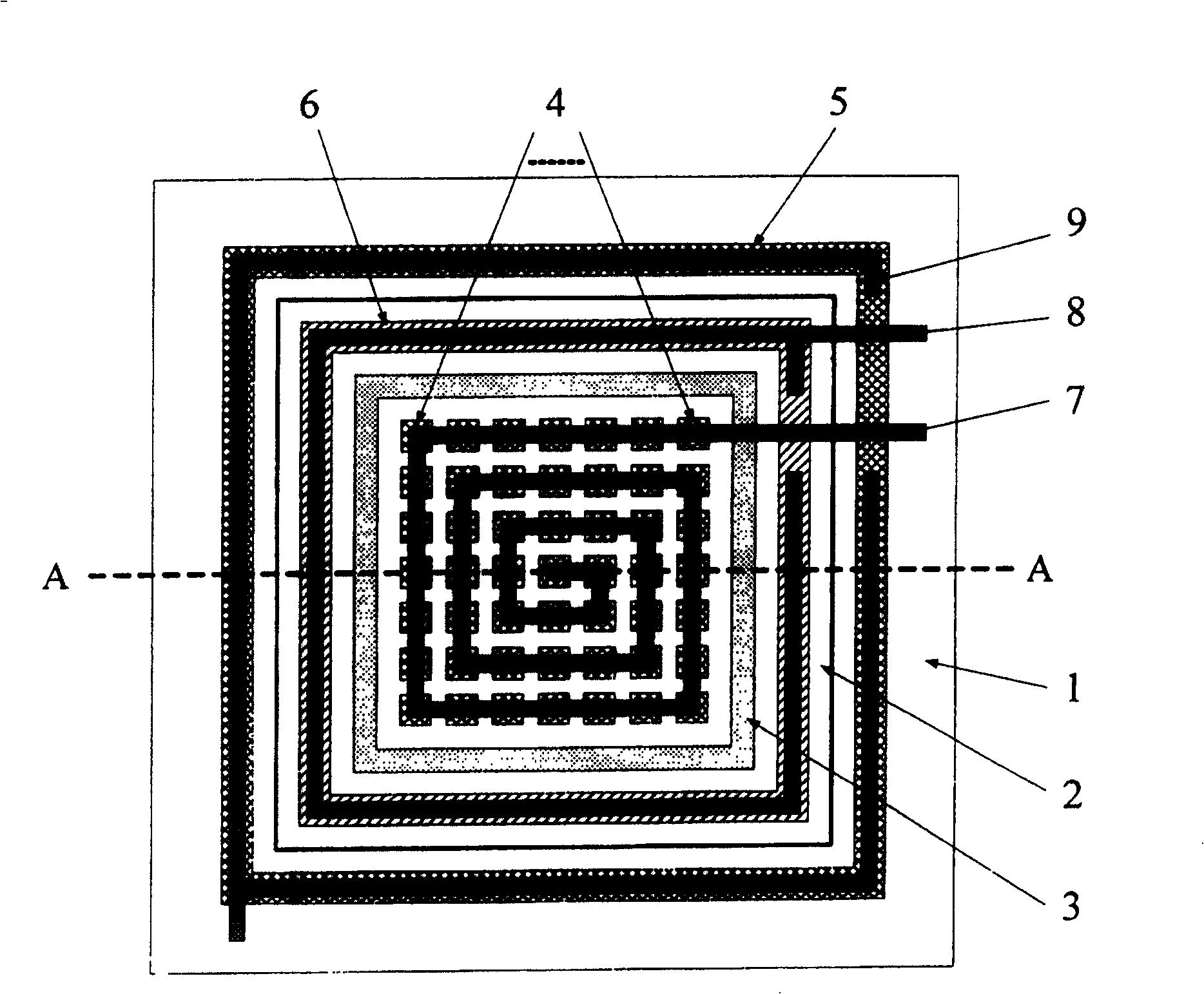
[0081] The production technology used for the photodetector designed in the present invention is all provided by the deep submicron CMOS technology, without any special requirements on the technology. Further set forth the present invention below in conjunction with embodiment and accompanying drawing:

[0082] 1. Fabricate an N well 2 with an area of ​​70 μm×70 μm on the P substrate 1 ; and prepare it simultaneously with the N well of the PMOS transistor. The depth is about 0.95μm, and the injection concentration is about 1×10 17 cm -3 .

[0083] 2. Forming an annular shallow trench isolation region 3 in the N well region 2 . The depth is about 0.8 μm, the width of the ring is 1 μm, and the outer edge of the ring is 3.5 μm away from the edge of the N well region 2 .

[0084] 3. Fabricate the array-shaped first P+ region 4 in the N well region 2 . Doping concentration is about 1×10 20 cm -3 . The array size is 7×7, the area of ​​each unit in the array is 6 μm×6 μm, and...


PUM


Abstract

The photo detector includes following parts: a P substrate; a quadratic N trap area prepared on P substrate; being prepared on N trap area, an annular shallow-channel isolation area is encircled by annular N trap area; being prepared on N trap area, a P+ region is encircled by annular shallow-channel isolation area so as to constitute anode of photo detector array; being prepared on N trap area, an annular N+ area is encircles the shallow-channel isolation area; being prepared on P substrate, an annular second P+ encircles the quadratic N trap area; a plane spiral metal electrode connects each unit block in array form one by one in first P+ area; an annular metal electrode is connected to N+ area; a annular metal electrode is connected to second P+ area.

Description

technical field [0001] The invention relates to a semiconductor optoelectronic device, in particular to a silicon-based photodetector structure fully compatible with deep submicron standard complementary metal oxide semiconductor (CMOS, Complementary Metal Oxide Semiconductor) technology and a manufacturing method thereof. Background technique [0002] The development of information technology means that information with larger capacity needs to be transmitted at a higher rate. However, the traditional metal interconnection is affected by various parasitic effects and cannot meet the transmission requirements of higher speeds. Optical interconnection is undoubtedly an ideal substitute technology. Using standard CMOS technology to realize photodetectors can directly interconnect optoelectronic devices with CMOS integrated circuits on the same chip, which can not only eliminate the adverse effects of various metal interconnections in hybrid integration, but also give full play...

Claims


Application Information

Patent Timeline
Patent Type & Authority Patents(China)
IPC IPC(8): H01L27/14H01L31/00H01L21/822
Inventor 陈弘达高鹏顾明刘海军
Owner INST OF SEMICONDUCTORS - CHINESE ACAD OF SCI
Why Eureka
Try Eureka