Air flow distribution equalized etching apparatus

A technology of uniform distribution and etching device, which is applied in the field of microelectronics, can solve the problems of uneven air flow, inhomogeneity, air flow obstruction, etc., and achieve the effect of uniform air flow distribution, small difference in chemical reaction speed, and good uniformity

Active Publication Date: 2008-07-02
BEIJING NAURA MICROELECTRONICS EQUIP CO LTD
View PDF5 Cites 0 Cited by
  • Summary
  • Abstract
  • Description
  • Claims
  • Application Information

AI Technical Summary

Problems solved by technology

However, because the supporting arm 3a has certain strength requirements and the inner cavity needs to pass through various electrical and mechanical pipelines such as the electrode rod 3b, the lower electrode pipeline 3c, etc., the volume is relatively large
As shown in Figure 3, the width of the lower electrode support arm 3a is relatively large, which inevitably hinders the airflow and forms a barrier on the path of the airflow, thereby affecting the symmetry of the airflow. figure 2 Among them, the gas flow encounters a barrier at the gas flow 4a, but the gas flow flows smoothly at the gas flow 4b. The gas flow at these two places is not uniform, and the gas flow is not uniform near the edge of the wafer 1, which is not conducive to the uniformity of the plasma.

Method used


Image

  • Air flow distribution equalized etching apparatus
  • Air flow distribution equalized etching apparatus
  • Air flow distribution equalized etching apparatus

Examples


Embodiment Construction

[0027] The specific implementation of the etching device with uniform gas flow distribution of the present invention will be further described in detail below in conjunction with the accompanying drawings, but it is not used to limit the protection scope of the present invention.

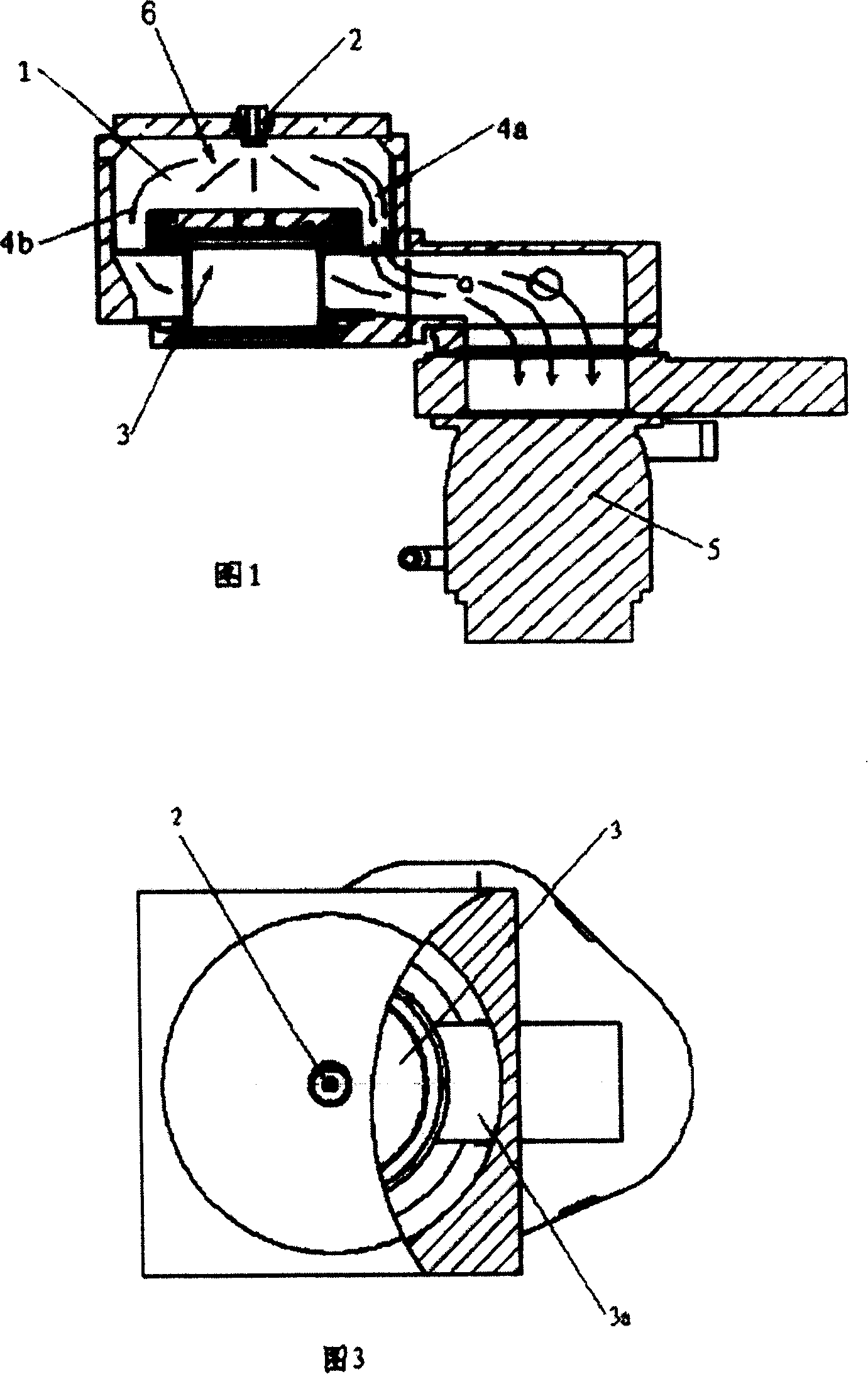
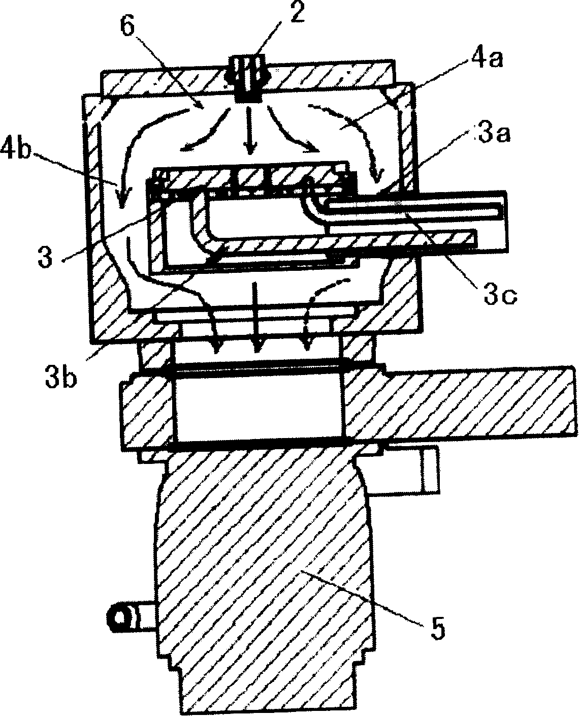
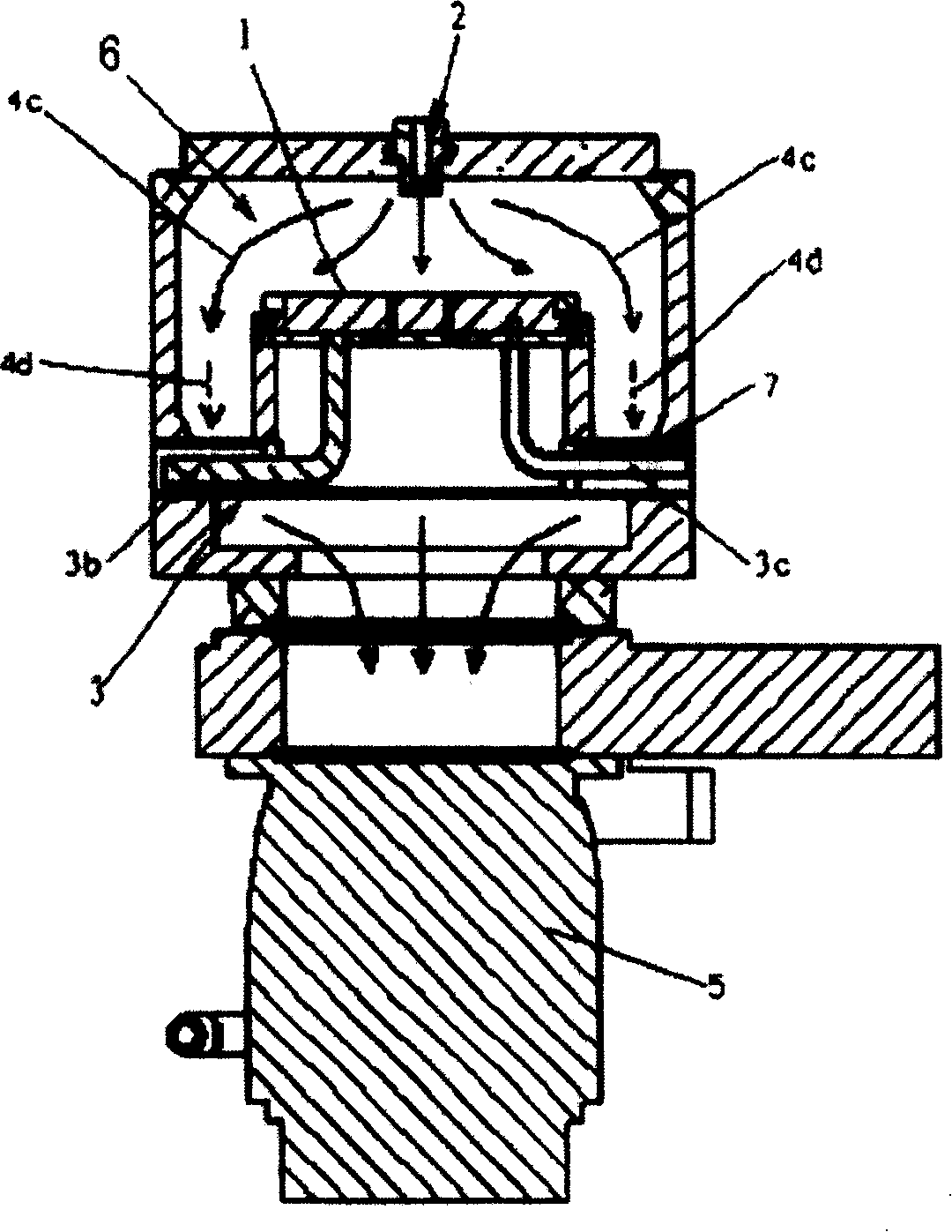
[0028] see Figure 4 , Figure 5 and Figure 6. The structure of the first embodiment of the etching device with uniform gas flow distribution of the present invention includes a reaction chamber 6 and a pumping chamber directly below the reaction chamber 6 . An air inlet device 2 is provided at the center of the top wall of the reaction chamber 6, and an air pumping device, namely a molecular pump 5, is provided at the bottom wall of the pumping chamber. An electrostatic chuck is installed in the center of the reaction chamber 6, and the wafer 1 to be processed is adsorbed on the electrostatic chuck, and a lower electrode device 3 is arranged below the electrostatic chuck, and the lower electrode ...


PUM


Abstract

The related etching device in semiconductor wafer processing comprises a reaction chamber and a lower electrode supporting device composed by even symmetrical-distributed connecting sleeves. The benefits of this invention include: well symmetry of the airflow upper the wafer, little effect to the upper airflow, good acceleration function to uniform field formed by plasma, and better evenness for chemical reaction speed and etching rate.

Description

technical field [0001] The invention relates to the technical field of microelectronics, in particular to an etching device in semiconductor wafer processing. Background technique [0002] The plasma etching machine mainly works by using the physical and chemical reactions of the plasma on the wafer. The uniformity of wafer etching is an extremely important index of the etching process, and closely related to this index is the gas flow field formed after the chemical gas enters the reaction chamber. The symmetry of the gas flow field relative to the center of the wafer is an inevitable requirement of the etching process, and is also a key technology that must be considered in the overall design of the etching machine reaction chamber. The gas flow field is mainly related to the gas injection device, the lower electrode device, and the air extraction device (molecular pump). Explanation of related technical terms: Airflow field: Since the plasma etching machine needs to mai...

Claims


Application Information

Patent Timeline
Patent Type & Authority Patents(China)
IPC IPC(8): H01L21/00H01L21/3065C23F1/12C23F4/00
Inventor 孙亚林
Owner BEIJING NAURA MICROELECTRONICS EQUIP CO LTD
Why Eureka
Try Eureka