Design method for cross section corrected bending optical waveguide structure
A design method and technology of optical waveguide, applied in the direction of optical waveguide light guide, cladding fiber, etc., can solve the problem of large optical bending loss, and achieve the effect of reducing optical loss, reducing external leakage, and improving transmission efficiency
- Summary
- Abstract
- Description
- Claims
- Application Information
AI Technical Summary
Problems solved by technology
Method used
Image
Examples
Embodiment Construction
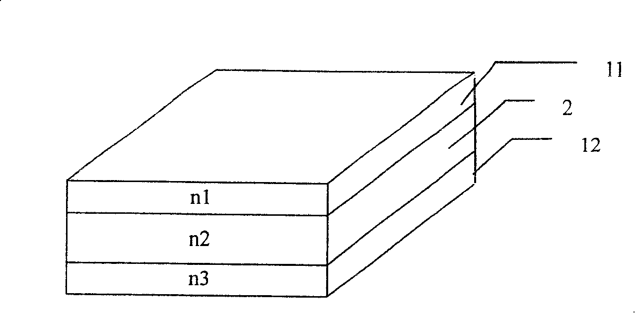
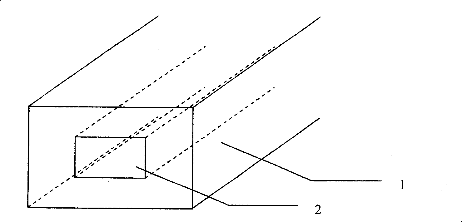
[0015] The design method of the present invention is that the thickness or height of the core layer on the outer side of the curved optical waveguide is always greater than that on the inner side of the optical waveguide, or the thickness or height on the curved surface is increased. The refractive index of the core layer 2 is greater than that of the cladding layer 1 . When the curved optical waveguide is a planar structure, the cladding layer 1 includes an upper cladding layer 11 and a lower cladding layer 12, the core layer 2 is located between the upper cladding layer 11 and the lower cladding layer 12, and the refractive index of the core layer 2 is greater than that of the upper cladding layer 11. or the refractive index of the lower cladding layer 12 .
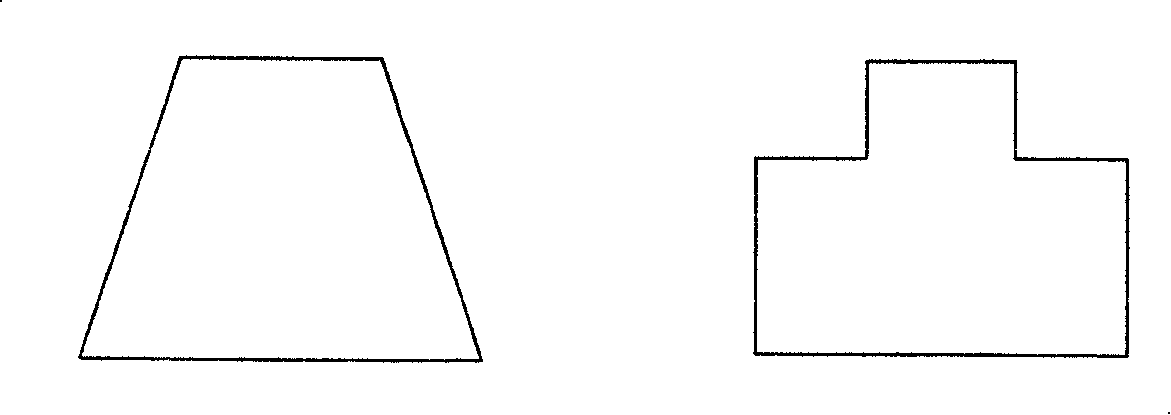
[0016] Schematic diagram of the structural design of the above section correction ( Figure 4 ), just illustrate the design method of the present invention, can not exhaust the whole of the figure designed by this meth...
PUM
 Abstract
Description
Claims
Application Information
 - R&D
- Intellectual Property
- Life Sciences
- Materials
- Tech Scout
- Unparalleled Data Quality
- Higher Quality Content
- 60% Fewer Hallucinations
Browse by: Latest US Patents, China's latest patents, Technical Efficacy Thesaurus, Application Domain, Technology Topic, Popular Technical Reports.
© 2025 PatSnap. All rights reserved.Legal|Privacy policy|Modern Slavery Act Transparency Statement|Sitemap|About US| Contact US: help@patsnap.com


