Image sensor and reader

An image sensing device and image information technology, applied in image communication, radiation control devices, televisions, etc., can solve problems such as the difficulty of designing CIS substrates

Inactive Publication Date: 2008-05-28
CANON KK
View PDF6 Cites 0 Cited by
  • Summary
  • Abstract
  • Description
  • Claims
  • Application Information

AI Technical Summary

Problems solved by technology

[0006] However, in order to further increase the resolution and speed of the CCD, as mentioned above, it is necessary to reduce the crosstalk of the multi-stage output and prevent the digital noise from being superimposed on the analog signal. With the conventional wiring technology, it is very difficult to design the CIS substrate.

Method used


Image

  • Image sensor and reader
  • Image sensor and reader
  • Image sensor and reader

Examples


Embodiment Construction

[0023] Hereinafter, preferred embodiments to which the present invention is applied will be described in detail with reference to the drawings.

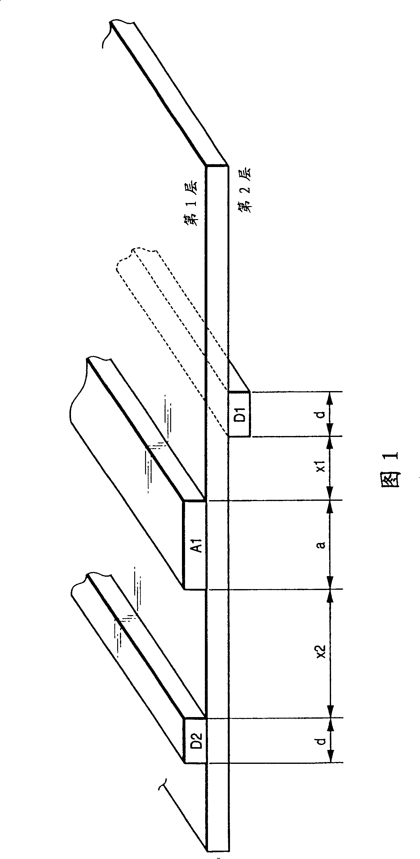
[0024] 1. The overall structure of the close-fitting image sensor

[0025] The overall structure of the adhesive image sensor used in this embodiment will be described with reference to FIG. 4 .

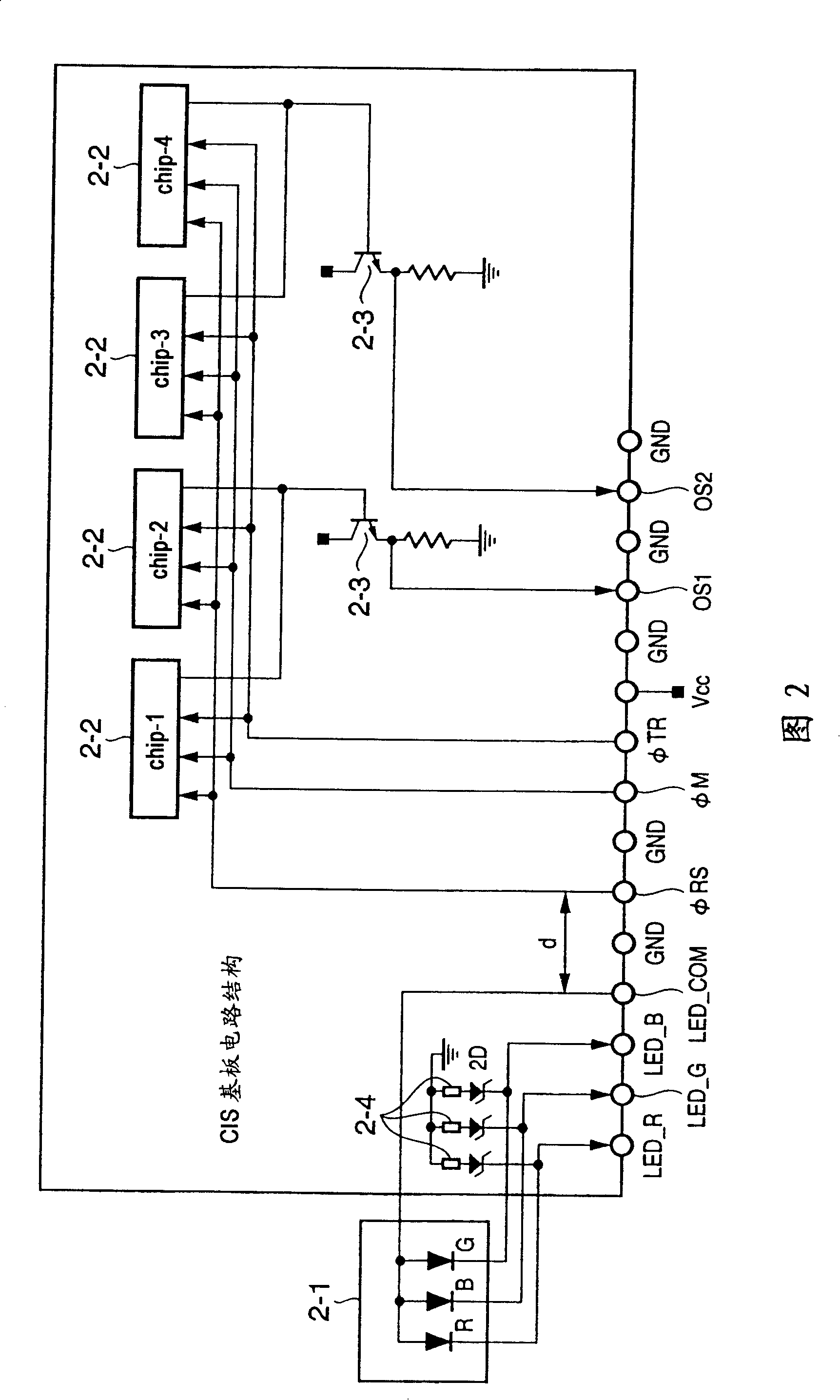
[0026] 4-1 is a linear light source unit, a light guide 4-1-2 that uniformly diffuses the light emitted from the light source unit along the reading main scanning direction by the LED light source unit 2-1 arranged at the end of the light source unit constitute.

[0027] The irradiated light irradiated from the light guide 4-1-2 is reflected by the original on the original glass, and the reflected light passes through the self-focusing lens array 4-2 to the photosensitive element (CCD) 2-3 fixed on the substrate 4-3. on the imaging.

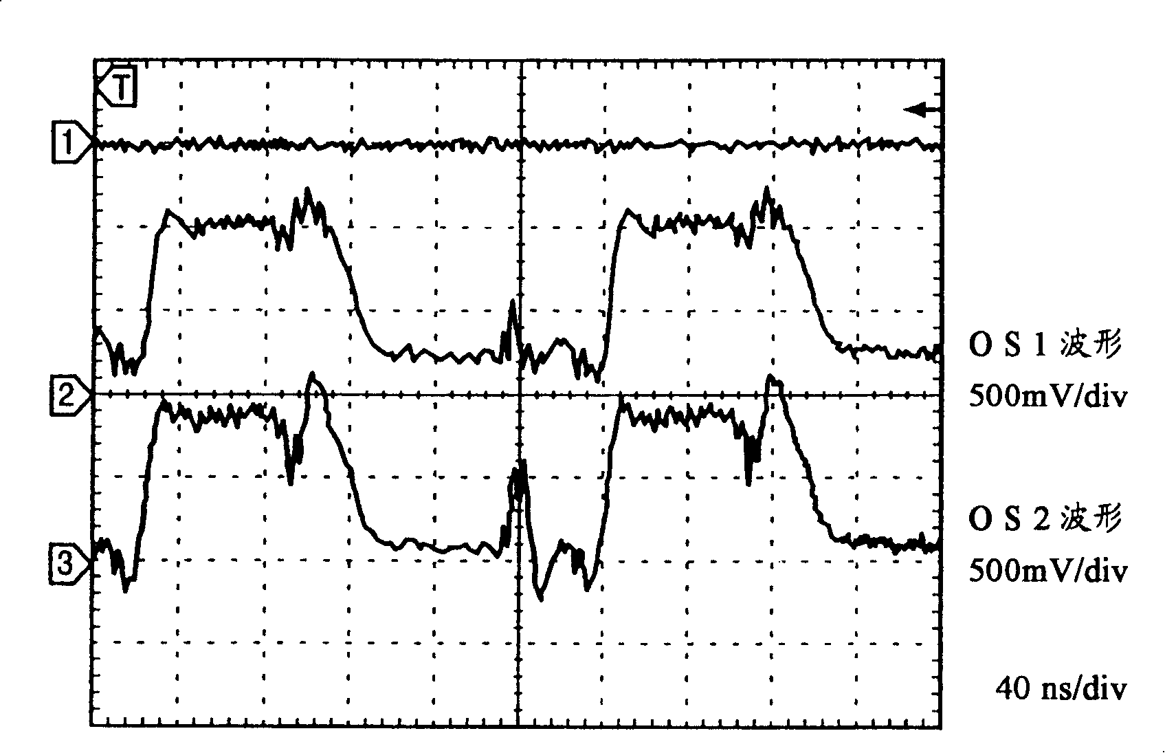
[0028] The imaged light is photoelectrically converted by CCD2-3, and sequentially output as image signa...


PUM


Abstract

It is an object of the present invention to provide wiring pattern conditions for obtaining a high-quality analog image output signal in a contact image sensor which operates at a high speed (5 MHz or more). In order to achieve this object, a CIS substrate has the following arrangement. Signal lines phiM, phiRS, and phiTR which transmit signals to CCD chips (2-2) are digital signal lines Dn, and signal lines from the CCD chips (2-2) to the inputs of emitter followers and output lines from the emitter followers are analog signal lines An. In FIG. 1, letting A1 be an analog signal line from the CCD, and D1 be a digital signal line, the analog signal line A1 and digital signal line D1 are formed on separate layers.

Description

technical field [0001] The present invention relates to an image sensor device and a reading device, and particularly relates to a wiring structure of an adhesive image sensor driven at high speed (5 MHz or higher). Background technique [0002] The contact image sensor (hereinafter referred to as CIS: Contact Image Sensor) can be miniaturized and low in power consumption according to its structure. , so it has a structure in which multiple CCD chips are arranged in a row. Furthermore, due to the low voltage of the photoelectric conversion chip, the range of the image signal as an analog signal is 1V for the voltage of the driving signal (usually 5V logic). The rate needs to be such high precision that 1LSB bit = about 4mV. Therefore, it is difficult to drive the conventional CIS at a high speed, and the driving frequency of the CCD chip is generally 1 to 2 MHz. [0003] Currently, there are increasing demands for performance improvement of image reading devices (requirem...

Claims


Application Information

Patent Timeline
Patent Type & Authority Patents(China)
IPC IPC(8): H04N1/00H04N1/04H04N1/40H04N1/047H01L27/14H01L27/146H01L27/148H01L29/04H01L31/062H04N1/028H04N1/03H04N1/031H04N5/222H04N25/00
CPCH01L27/14806Y10S257/929H01L27/14678
Inventor 小泉和久
Owner CANON KK
Why Eureka
Try Eureka