Interface modular converter and method for configuration of FPGA

A technology for interface conversion and configuration data, which is applied to instruments, electrical digital data processing, etc., can solve problems such as increased software complexity, occupied bridge I/O resources, poor versatility, etc., and achieves improved flexibility and module compatibility Good performance, improved configuration speed and reliability

Active Publication Date: 2008-05-14
ZTE CORP
View PDF5 Cites 1 Cited by
  • Summary
  • Abstract
  • Description
  • Claims
  • Application Information

AI Technical Summary

Problems solved by technology

[0004] However, in products based on Intel's X86 architecture as the processor platform, the processor does not have general-purpose I / O pins that can be connected to the FPGA, although it can be connected to the FPGA through the I / O of the bridge chip, and the bridge chip can be controlled by software The I / O analog configuration timing sequence of the FPGA is downloaded, but this not only occupies the I / O resources of the bridge, but also has poor flexibility (because the fixed I / O pins of the bridge are required), and the versatility is not good (because different bridges I / O definitions are not necessarily the same), and the configuration speed is slow, the complexity of the software increases, and the reliability decreases

Method used


Image

  • Interface modular converter and method for configuration of FPGA
  • Interface modular converter and method for configuration of FPGA
  • Interface modular converter and method for configuration of FPGA

Examples


Embodiment Construction

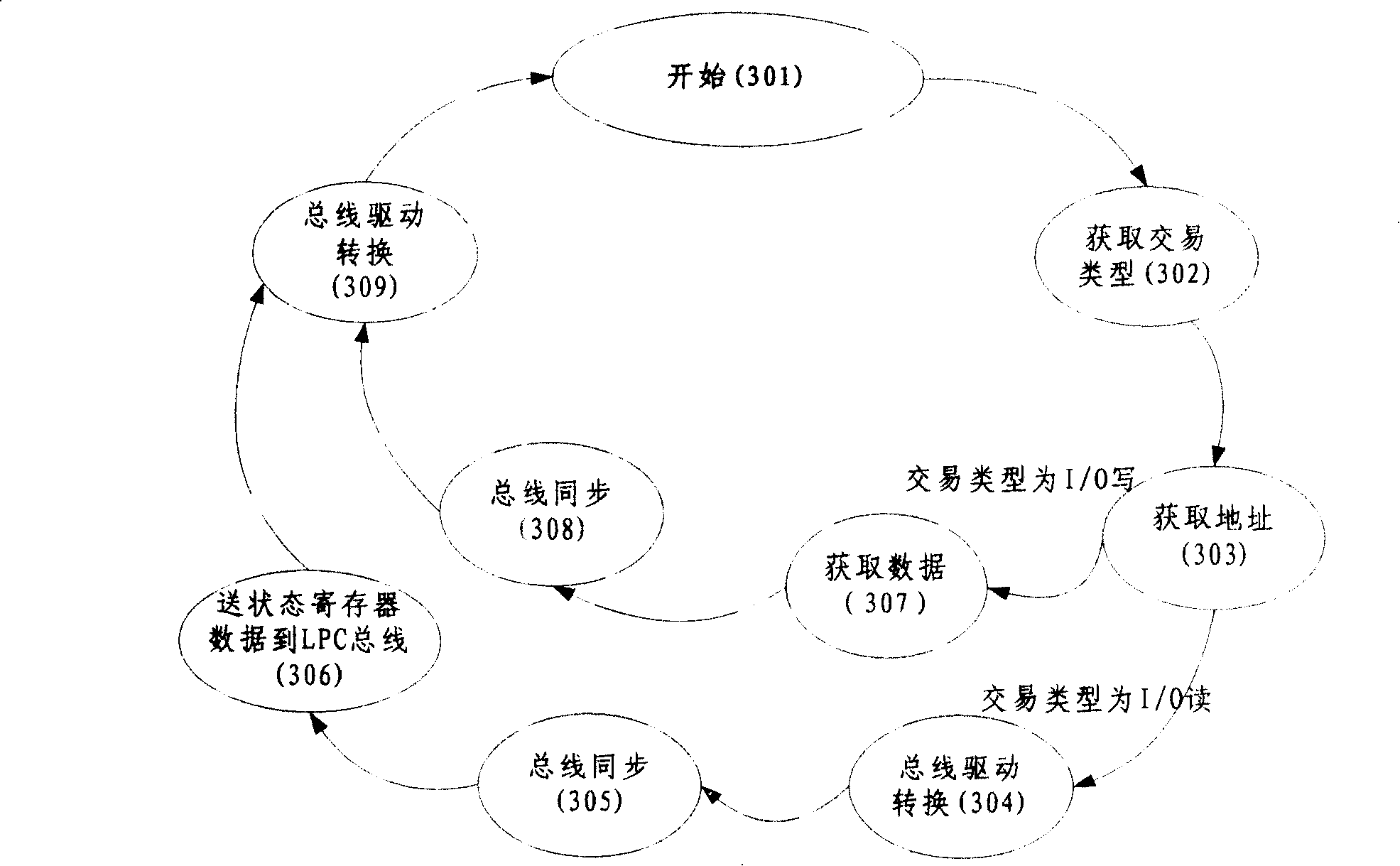
[0019] Below in conjunction with accompanying drawing, the implementation of technical scheme is described in further detail:

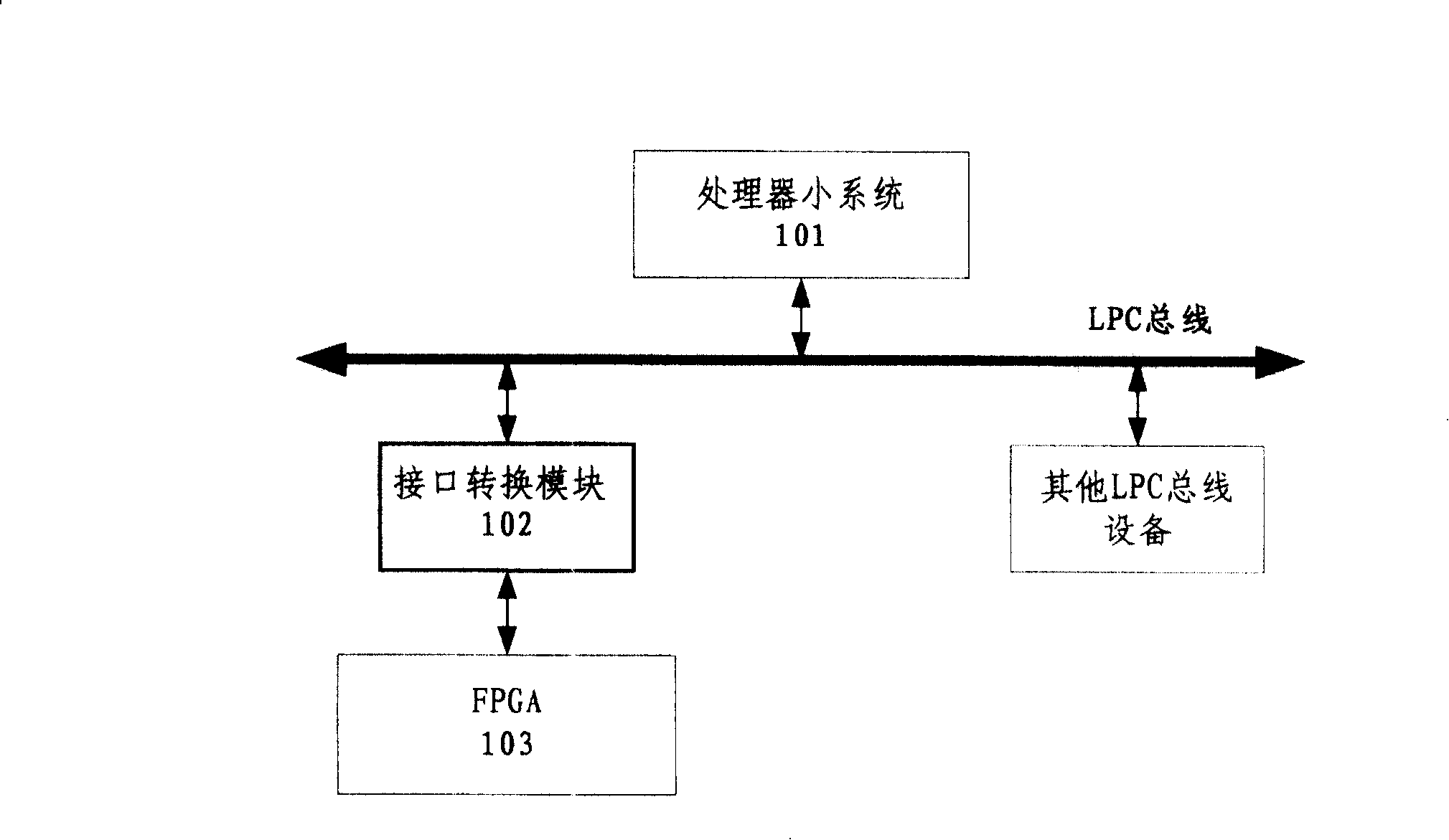
[0020] Such as figure 1 Shown, the structural block diagram of application environment system of the present invention, this system comprises:

[0021] The small processor system 101 may include a processor, a memory, a bridge chip, and a BIOS, etc., and is an independent processor system that can run programs, and can run an operating system and configuration programs in the present invention.

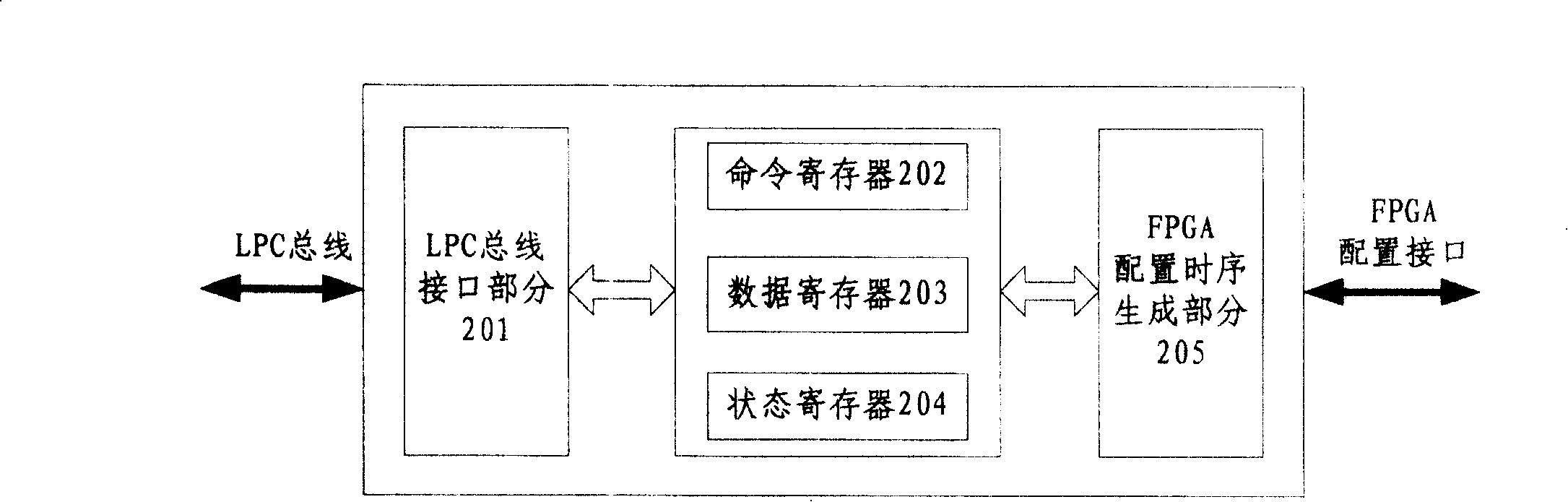
[0022] The interface conversion module 102, this module is hung on the LPC bus as an LPC bus device, and completes the timing conversion function from the LPC bus to the FPGA serial configuration, and the processor completes the online configuration of the FPGA through this module. The block diagram of the internal structure of the hardware module is as follows: figure 2 As shown, it mainly includes an LPC bus interface part 201, a register set (202-204) a...


PUM


Abstract

This invention relates to an interface switch module and a method for configuring FPGA, in which, the interface switch module includes a LPC bus interface part, an order register, a data register, a state register and a FPGA configuration time sequence generation part. The method includes: the processor starts a configuration instruction via the LPC bus to the interface switch module to generate the initialized time sequence downloaded by the FPGA to be initialized, sending the configuration data via the LPC to the interface switch module to generate the FPGA download time sequence to download the data to FPGA, sending the configuration ending order to the interface switch module to generate relative configuration ending time sequence or the module finishes relative configuration ending time sequence after the data are configured.

Description

technical field [0001] The invention relates to a method for configuring an FPGA, more specifically, a method for configuring an FPGA (field programmable gates array) on a circuit board through an LPC (Low Pin Count) bus. Background technique [0002] In order to facilitate the on-site upgrade of products and reduce the cost of dedicated PROM (Programmable Read-Only Memory programmable read-only memory) chips used to configure FPGAs, many products require that the FPGA on the circuit board can be configured online through the CPU (processor). [0003] Under normal circumstances, the I / O (input and output) pins of the processor are generally directly connected to the serial configuration pins of the FPGA, and the FPGA is configured by simulating the configuration timing of the FPGA through software. [0004] However, in products based on Intel's X86 architecture as the processor platform, the processor does not have general-purpose I / O pins that can be connected to the FPGA, ...

Claims


Application Information

Patent Timeline
Patent Type & Authority Patents(China)
IPC IPC(8): G06F13/38
Inventor 杨思远吴边邵贵阳孟春才段晓雪
Owner ZTE CORP
Why Eureka
Try Eureka