Lower-extraction type etching device

An etching device and gas-type technology, applied in the field of microelectronics, can solve problems such as large changes, no axial symmetry, and large differences in chemical reaction speeds, and achieve good uniformity

Active Publication Date: 2008-01-16
BEIJING NAURA MICROELECTRONICS EQUIP CO LTD
View PDF4 Cites 0 Cited by
  • Summary
  • Abstract
  • Description
  • Claims
  • Application Information

AI Technical Summary

Problems solved by technology

Due to the influence of the molecular pump, the flow velocity is fast on the side near the exhaust port 4, and the gas density is small, and the flow velocity is slow on the side away from the exhaust port 4, and the gas density is relatively high. The distribution above the surface does not have axial symmetry, and changes greatly on the surface of the electrostatic chuck, resulting in a large difference in the chemical reaction speed between the formed reactive groups and the surface of the etched material, which eventually leads to the inhomogeneity of the etching rate

Method used


Image

  • Lower-extraction type etching device
  • Lower-extraction type etching device

Examples


Embodiment Construction

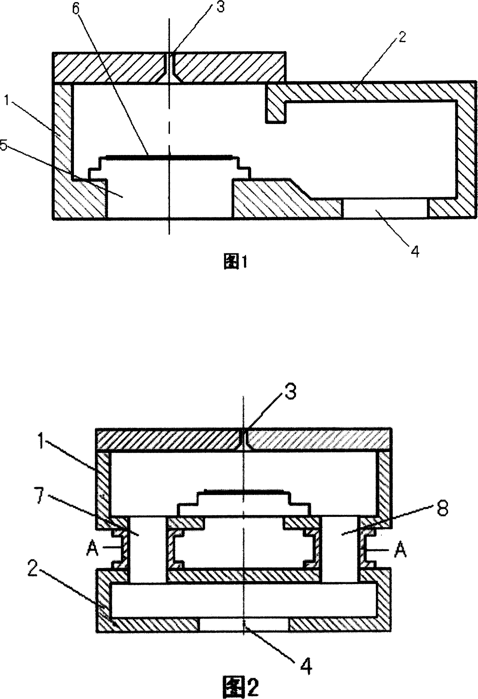
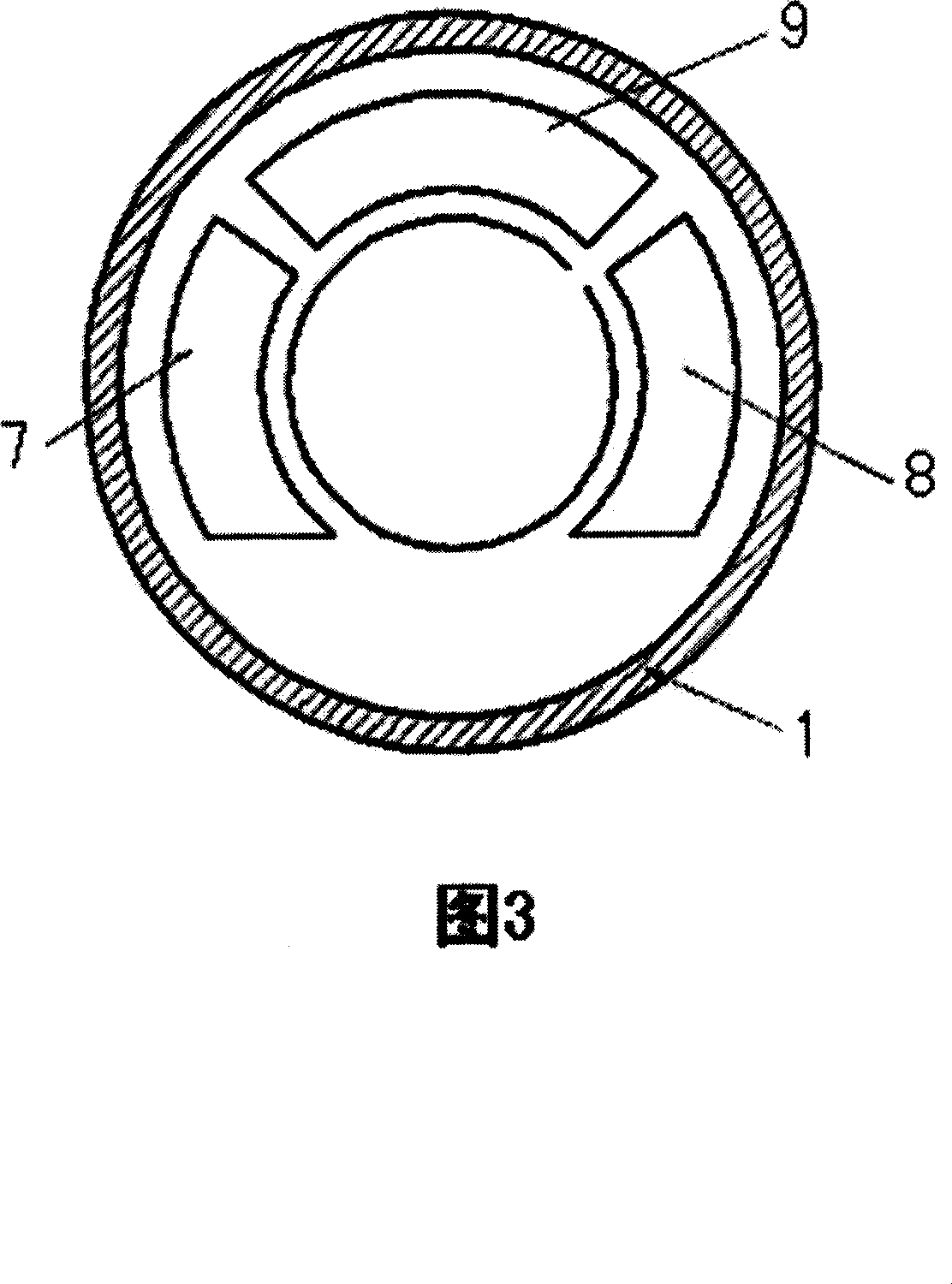
[0022] The specific implementation of the down pumping etching device of the present invention will be described in further detail below in conjunction with the accompanying drawings, but it is not used to limit the protection scope of the present invention.

[0023] See Figures 2 and 3. The down pumping etching device of the present invention includes a reaction chamber 1 with an air inlet 3 and an air pumping chamber 2 with an exhaust port 4 . Wherein the pumping chamber 2 is positioned at the below of the reaction chamber 1, and a rear exhaust channel 9 and a symmetrically arranged left exhaust channel 7 and a right exhaust channel 8 are connected between the two, the rear exhaust channel 9, the left exhaust channel The cross sections of the channel 7 and the right exhaust channel 8 are circular and concentric with the electrostatic chuck 5. The exhaust channel 9, the left exhaust channel 7 and the right exhaust channel 8 are connected with the reaction chamber 1 and the pu...


PUM


Abstract

This invention relates to an etching device in the process of semiconductor wafers including a reacting chamber with an inlet and a pumping chamber with an air vent, in which, said pumping chamber is set under the reacting chamber connected with symmetrically arranged left ventilation channel and a right ventilation channel and said air vent and the inlet are at the same axes and arranged symmetrically, so the gas above the static chuck surface flows to either side symmetrically and realizes uniform pumping to the reacting chamber.

Description

technical field [0001] The invention relates to the technical field of microelectronics, in particular to an etching device in semiconductor wafer processing. Background technique [0002] Under low pressure, the reaction gas is excited by radio frequency power to generate ionization to form plasma. The plasma is composed of charged electrons and ions. Under the impact of electrons, the gas in the reaction chamber can not only transform into ions, but also absorb energy and form a large number of active groups. The active reactive groups react chemically with the surface of the etched substance and generate volatile reaction products. The reaction product breaks away from the surface of the material to be etched and is drawn out of the cavity by the vacuum system. A non-uniform gas distribution within the reaction chamber will result in large variations in etch rate and uniformity across the wafer surface inside the chamber. In a semiconductor fabrication plant, the proce...

Claims


Application Information

Patent Timeline
Patent Type & Authority Patents(China)
IPC IPC(8): H01L21/00H01L21/3065H01L21/67C23F4/00
Inventor 张之山
Owner BEIJING NAURA MICROELECTRONICS EQUIP CO LTD
Why Eureka
Try Eureka