Dynamic random access storage unit and its manufacturing method
A dynamic random access and memory cell technology, applied in semiconductor/solid-state device manufacturing, electrical components, transistors, etc., can solve problems such as the inability of capacitors to shrink, achieve high capacitive coupling rate, avoid leakage, and reduce manufacturing costs.
- Summary
- Abstract
- Description
- Claims
- Application Information
AI Technical Summary
Problems solved by technology
Method used
Image
Examples
Embodiment Construction
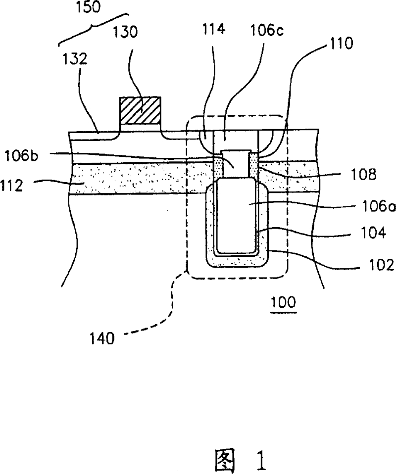
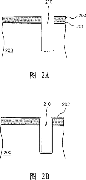
[0042] 2A to 2H are schematic cross-sectional views of a manufacturing process of a dynamic random access memory unit (DRAM cell) according to a preferred embodiment of the present invention, which can be applied to a system-on-chip (SOC). Referring to FIG. 2A , a substrate 200 such as a silicon substrate is provided, a pad oxide 201 is formed on the substrate 200 , and a mask layer 203 is formed on the pad oxide 201 . Afterwards, using the mask layer 203 as a mask, a trench 210 is formed in the substrate 200 by etching.
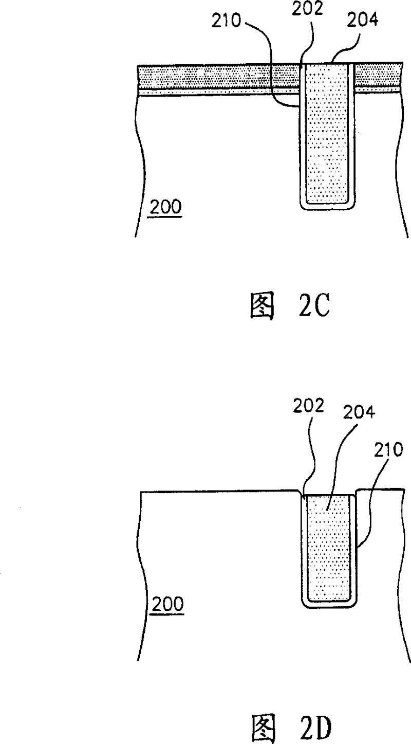
[0043] Next, referring to FIG. 2B , a capacitive dielectric layer 202 is formed on the substrate 200 to cover the surface of the trench 210 . The capacitor dielectric layer 202 is, for example, a silicon oxide / silicon nitride / silicon oxide stack layer (ONO) or a silicon nitride / silicon oxide stack layer (NO).
[0044]Subsequently, referring to FIG. 2C , a first conductive layer 204 is formed in the trench 210 , wherein the material of the first conductive l...
PUM
 Abstract
Description
Claims
Application Information
 - Generate Ideas
- Intellectual Property
- Life Sciences
- Materials
- Tech Scout
- Unparalleled Data Quality
- Higher Quality Content
- 60% Fewer Hallucinations
Browse by: Latest US Patents, China's latest patents, Technical Efficacy Thesaurus, Application Domain, Technology Topic, Popular Technical Reports.
© 2025 PatSnap. All rights reserved.Legal|Privacy policy|Modern Slavery Act Transparency Statement|Sitemap|About US| Contact US: help@patsnap.com


