Plane displaying device structure

A device structure and flat-panel display technology, which can be applied to identification devices, static indicators, instruments, etc., can solve the problems of limited signal conversion curve range, the quality of flat-panel display devices cannot be further improved, and the luminous brightness of light-emitting components is not as expected, so as to achieve quality Enhanced effect

Active Publication Date: 2007-12-05
AU OPTRONICS CORP
View PDF4 Cites 0 Cited by
  • Summary
  • Abstract
  • Description
  • Claims
  • Application Information

AI Technical Summary

Problems solved by technology

[0007] Although the above-mentioned adjustment unit can adjust the signal conversion curve, when the variable resistor is used for adjustment, the range that can change the signal conversion curve is limited
In the process of actually manufacturing flat-panel display devices, due to the drift effect, the threshold voltage values ​​between the gate and drain of the thin-film transistors of each flat-panel display device are different, so even if the same signal is input to the gate of the thin-film transistor poles, the output currents to the light-emitting components are also different, resulting in the luminous brightness of the light-emitting components will not be as expected
Since the difference in the threshold voltage value is determined by the environmental conditions during actual production, sometimes the error may exceed 1 volt, so that the range of the signal conversion curve that can be adjusted by the existing adjustment unit cannot correct such a large error, which causes the brightness of the display device to be inferior. As expected, the quality of flat-panel display devices cannot be further improved
[0008] In view of the above situation, the present invention provides a structure of a flat panel display device, which includes an adjustment unit, which can adjust the signal conversion curve by a large vertical translation, so as to solve the problem of insufficient amplitude of the adjustment signal conversion curve of the existing known adjustment unit

Method used


Image

  • Plane displaying device structure
  • Plane displaying device structure
  • Plane displaying device structure

Examples


Embodiment Construction

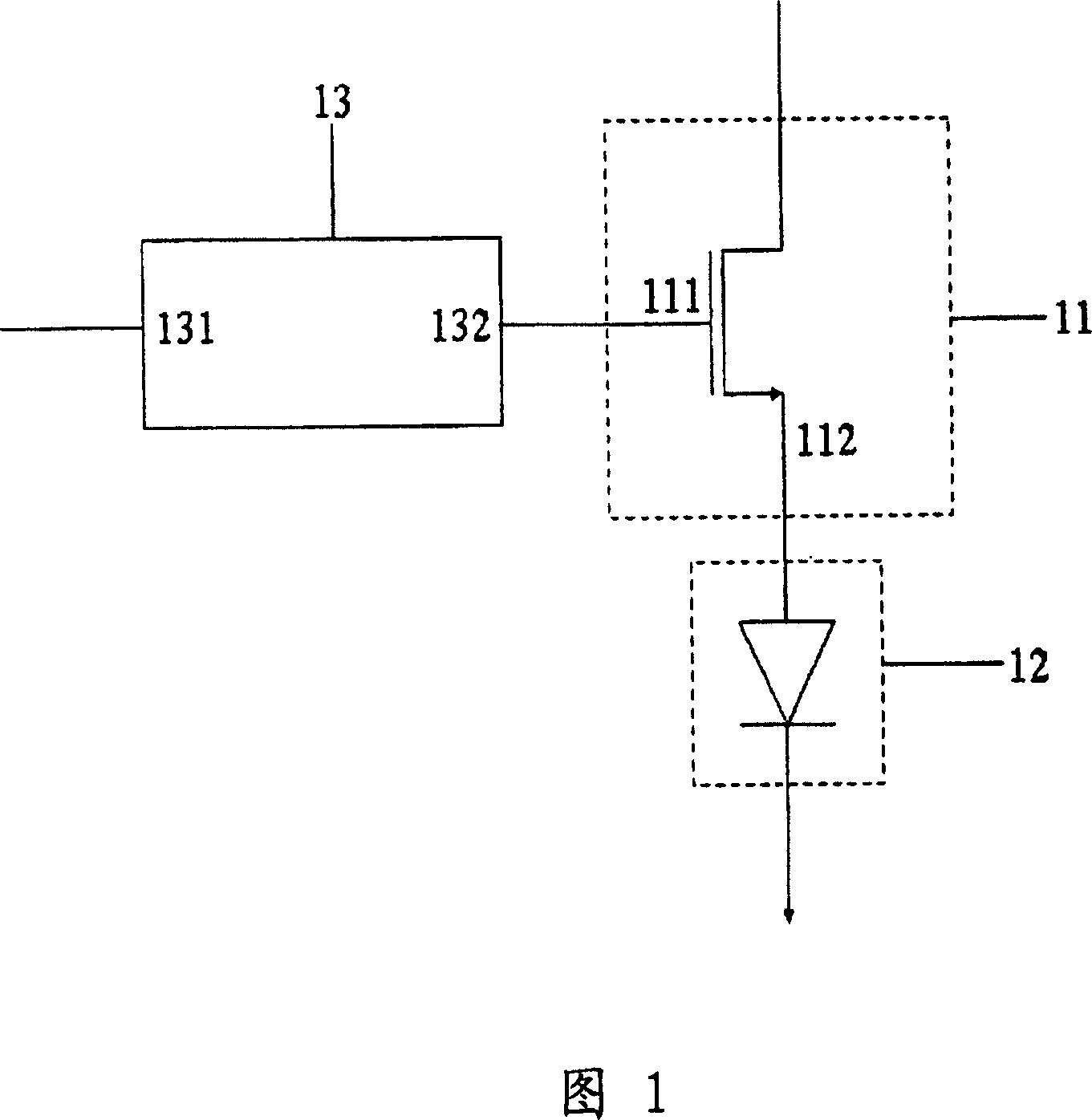
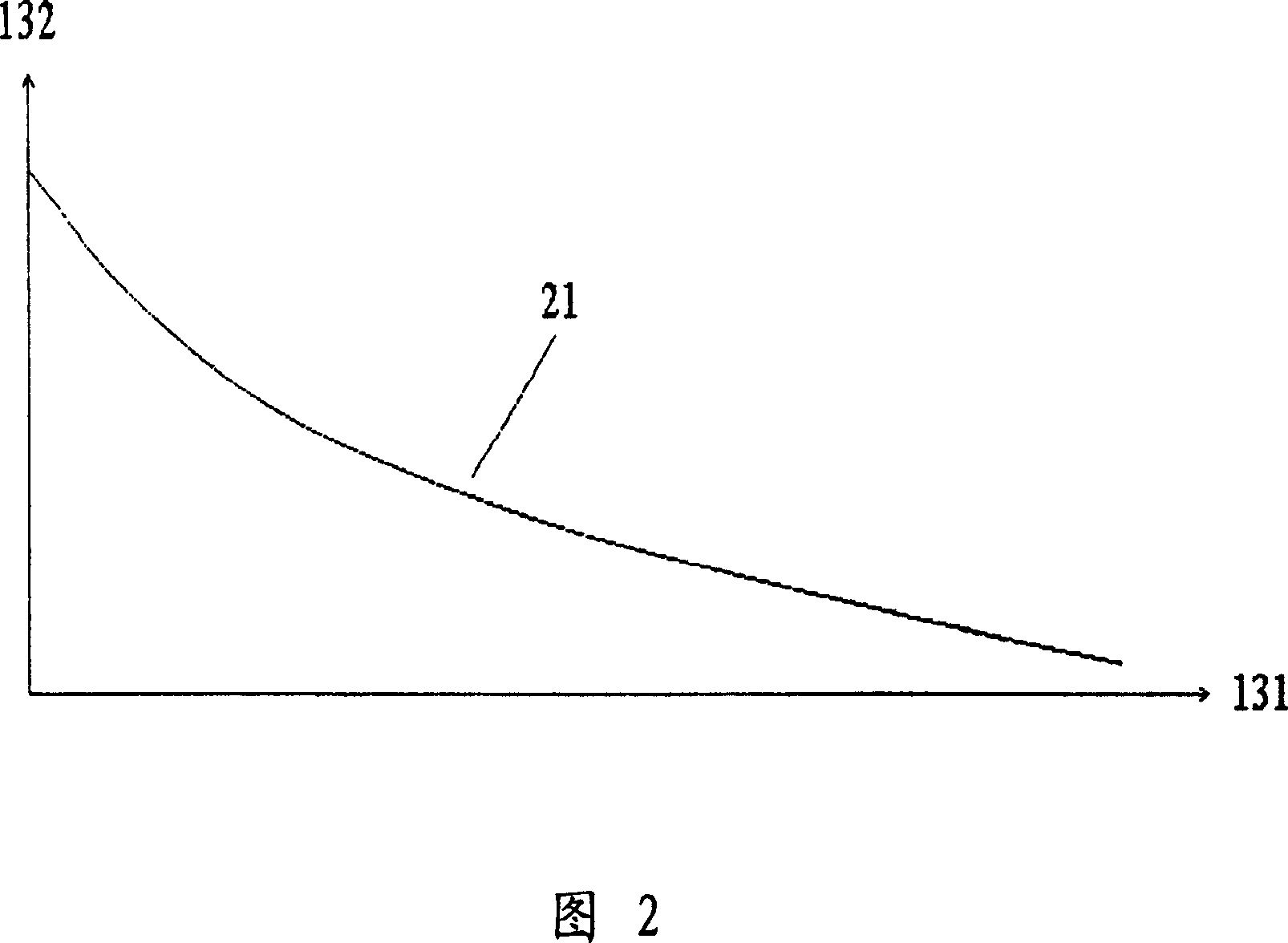
[0062]Please refer to FIG. 5 , which is a structural diagram of a flat panel display device according to the present invention, including a pixel 51 and an adjustment unit 52 , wherein the pixel 51 also includes a thin film transistor 511 and a light emitting component 512 and the drain of the thin film transistor 511 The electrode 5111 is connected in series with the light-emitting element 512 , and the output terminal of the adjustment unit 13 is connected to a gate 5112 of the thin film transistor 511 for signal. The user can change the output signal 522 through a signal conversion curve of the pixel 51 by changing the input signal 521 of the adjustment unit 52, and the thin film transistor 511 is connected between the gate 5112 and the drain 5111 according to the input signal of the gate 5112 The threshold voltage value determines the current input into the light-emitting component 512 through the drain 5111 . The luminance of the light-emitting component 512 , that is, th...


PUM


Abstract

The structure includes multiple pixels and an adjustment unit. The pixel includes a thin film transistor (TFT) and a luminescence module. TFT is connected to luminescence module in series. Signal of the adjustment unit is connected to one end of TFT. The adjustment unit makes a signal transformation curve carry out an adjustment action of vertical shift to adjust brightness of the pixel. Adjustment unit can use resistance voltage division or conversion circuit of DC voltage to reach adjustment purpose. Receiving high and low electrical level of external voltage signal, the adjustment unit realizes adjustment action of vertical shift for the signal transformation curve. The invention meets requirement for adjusting amplitude of signal transformation curve.

Description

technical field [0001] The present invention relates to a structure of a flat display device, in particular to a structure of a flat display device, which includes an adjustment unit for adjusting the pixel brightness of the structure of the flat display device. Background technique [0002] In recent years, flat-panel displays such as flat-screen TVs, mobile phones, personal digital assistants, digital cameras, car displays, and projectors have been widely used by the general public. [0003] Please refer to FIG. 1 , which is a known structure of a flat panel display device, including a thin film transistor 11 , a light emitting element 12 and an adjustment unit 13 . The output end of the adjustment unit 13 is signal-connected to a gate 111 of the TFT 11 , and a drain 112 of the TFT 11 is signal-connected to one end of the light-emitting element 12 . The user can change the output signal 132 through a signal conversion curve by changing the input signal 131 of the adjustme...

Claims


Application Information

Patent Timeline
Patent Type & Authority Patents(China)
IPC IPC(8): G09G3/32G09F9/33G09G3/3225
Inventor 胡硕修
Owner AU OPTRONICS CORP
Why Eureka
Try Eureka