Support entering into the fabrication of an electronic device, corresponding memory card connector, memory card read terminal and manufacturing method

a technology for supporting and electronic devices, applied in the field of electronic devices, can solve the problems of terminals which previously had little protection, terminals to be put out of operation, and large complexity of manufacture, and achieve the effect of increasing the height of the deposit and limiting the space requiremen

Active Publication Date: 2018-05-22
BANKS & ACQUIRERS INT HLDG
View PDF9 Cites 1 Cited by
  • Summary
  • Abstract
  • Description
  • Claims
  • Application Information

AI Technical Summary

Benefits of technology

[0033]It is thus possible to avoid the use of “fictitious” components whose function is limited to forming a physical protection barrier to protect “sensitive” components from fraudulent access aimed at damaging the electronic printed circuit board or the components mounted on the support.
[0085]Besides, a ratio of four or five between the width LDEP of said depositing surface of said permanent assembling material and the width Lo of said three-dimensional element increases the risk of appearance of conductive beads of assembling material.

Problems solved by technology

However, because of these standards, terminals which previously had little protection are gradually being replaced by increasingly secured terminals.
When an object tries to penetrate the protective enclosure, a short-circuit is produced, then causing the terminal to be put out of operation.
These efforts to set up protection have led to great complexity of manufacture, and the cost of manufacture has also increased.
In addition to the complexity of manufacture of the terminal, these methods make the maintenance of the terminals produced highly complex or even impossible, thus giving rise to many difficulties as much for the maintenance service providers as for the manufacturer of the memory card reading terminal.
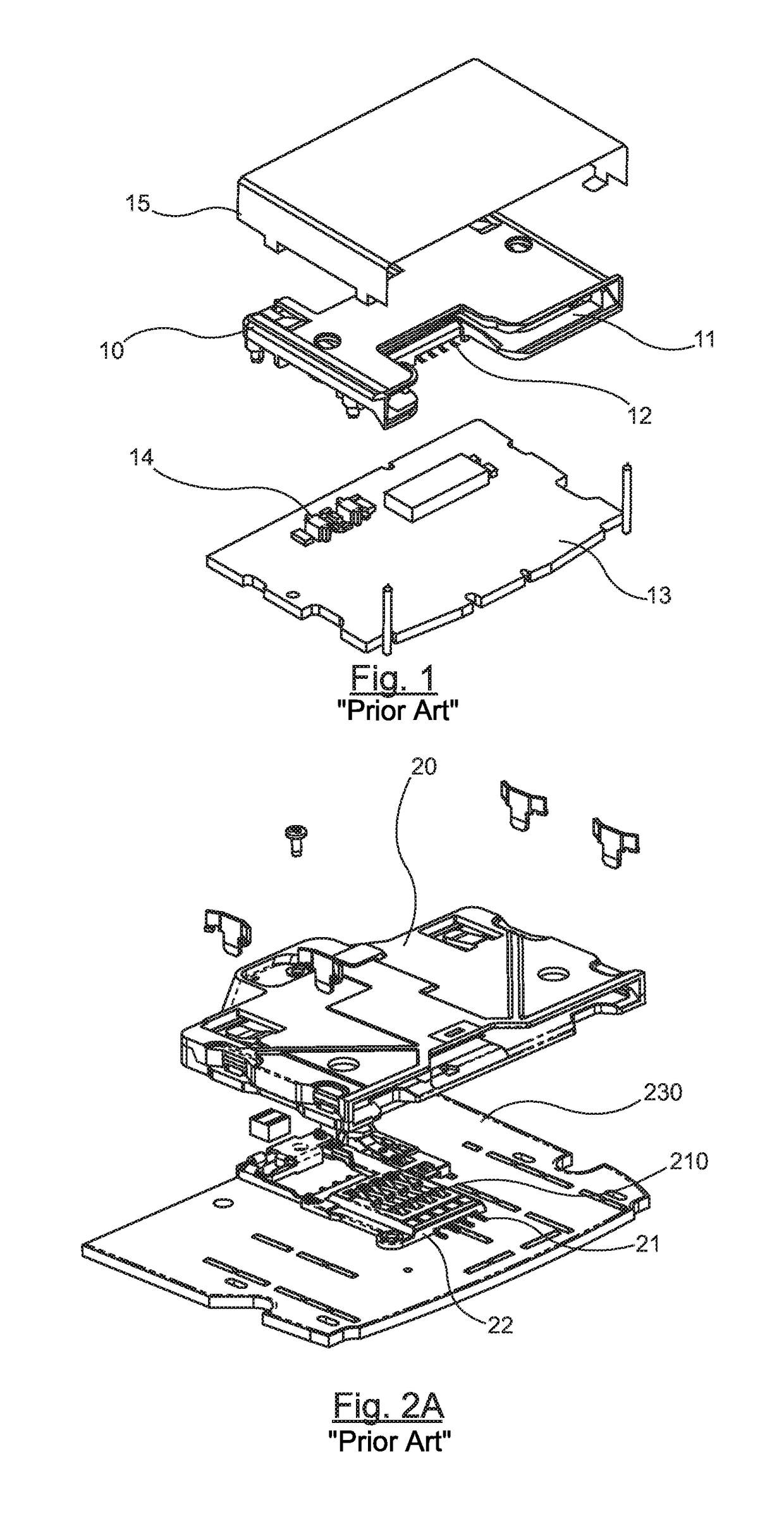
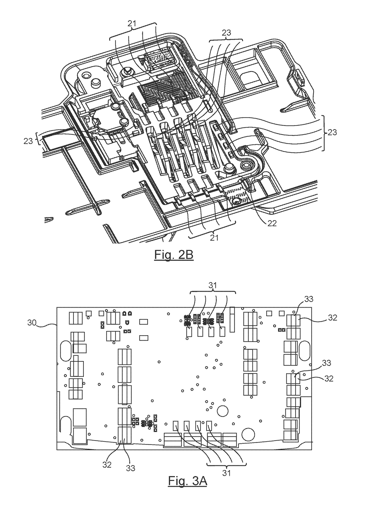
The drawback of the current technique lies in the need to solder these components 23, in proximity to the signal to be protected.
This requirement sometimes involves soldering defects or else solders of components (these components constituting the physical protection barrier, or again components in which the sensitive signals will travel) that become prone to damage because of successive steps of heat treatment.
These soldering defects or damage-prone solders are very difficult to detect and lead to difficulties of integration especially when one of the components gets unsoldered and therefore becomes mobile within the electronic device and therefore liable to cause deterioration of the electronic device.
This greatly increases the number of components 23 to be soldered and the drawbacks related to the soldering of such components.
In particular, such physical protection barriers based on the layout of the components 23 show poor resistance to climatic conditions.
Thus, such physical protection barriers based on the layout of the components also prove to be unnecessarily costly.

Method used


Image

  • Support entering into the fabrication of an electronic device, corresponding memory card connector, memory card read terminal and manufacturing method
  • Support entering into the fabrication of an electronic device, corresponding memory card connector, memory card read terminal and manufacturing method
  • Support entering into the fabrication of an electronic device, corresponding memory card connector, memory card read terminal and manufacturing method

Examples


Embodiment Construction

[0095]6.1 Reminder of the Principle of the Invention

[0096]The general principle of the technique described consists in modifying the constitution of a support comprising at least one component to be protected, in diverting a permanent assembling material from its classic use to form a three-dimensional element, the height of which is at least equal to the height of an electronic component, to act as a physical protection barrier for the component to be protected.

[0097]Such three-dimensional protective elements are therefore formed chiefly by a permanent assembling material that costs little and is easily available because it is also used classically to fixedly attach an electronic component to the support.

[0098]Thus, there is no obvious way to divert the function of a material classically used to fixedly attach two elements, namely for example a component and the support, in order to use it directly to form three-dimensional protection elements.

[0099]The general principle of the tec...


PUM

PropertyMeasurementUnit
heightaaaaaaaaaa
melting temperatureaaaaaaaaaa
heightaaaaaaaaaa

Abstract

A support is provided for fabrication of an electronic device. The support includes at least one component to be protected and at least one three-dimensional element of a height at least equal to a height of the electronic component. The three-dimensional element is disposed laterally opposite the at least one component to be protected. The three-dimensional element is chiefly constituted of a permanent assembling material.

Description

1. CROSS-REFERENCE TO RELATED APPLICATIONS[0001]This Application is a Section 371 National Stage Application of International Application No. PCT / EP2014 / 072821, filed Oct. 24, 2014, the content of which is incorporated herein by reference in its entirety, and published as WO 2015 / 062981 A1 on May 7, 2015, not in English.2. FIELD OF THE INVENTION[0002]The invention is situated in the field of electronics and more particularly that of the protection of signals travelling in a circuit, in a magnetic read head or again the protection of the balls of a ball grid array (BGA) corresponding to an integrated circuit pack to be soldered to a printed circuit board.[0003]The invention is therefore aimed at an application in the field of memory card readers or magnetic read head readers or readers comprising a BGA pack.[0004]According to one particular example, an object of the invention is a memory card reader comprising a memory card (MC) connector that is to be inserted into a magnetic card r...

Claims


Application Information

Patent Timeline
Patent Type & Authority Patents(United States)
IPC IPC(8): H05K7/00G06F21/86G06K7/00H05K1/02B23K1/00H05K3/34H05K3/10H05K3/24H05K3/12H05K3/14B23K101/42
CPCH05K1/0284G06F21/86G06K7/0091H05K1/0275H05K3/10H05K3/34B23K1/0016H05K2203/0551B23K2201/42H05K3/1241H05K3/1275H05K3/143H05K3/245H05K2201/098H05K2201/09409H05K2201/09781H05K2201/10204B23K2101/42
Inventor PAVAGEAU, STEPHANELAMBERT, XAVIER
Owner BANKS & ACQUIRERS INT HLDG
Why Eureka
Try Eureka