Cable connector and carrier module thereof
a carrier module and cable connector technology, applied in the direction of coupling contact members, coupling device connections, two-part coupling devices, etc., can solve problems such as unstable connection between positioning members and circuit boards, and achieve the effect of effectively solving problems
- Summary
- Abstract
- Description
- Claims
- Application Information
AI Technical Summary
Benefits of technology
Problems solved by technology
Method used
Image
Examples
first embodiment
[First Embodiment]
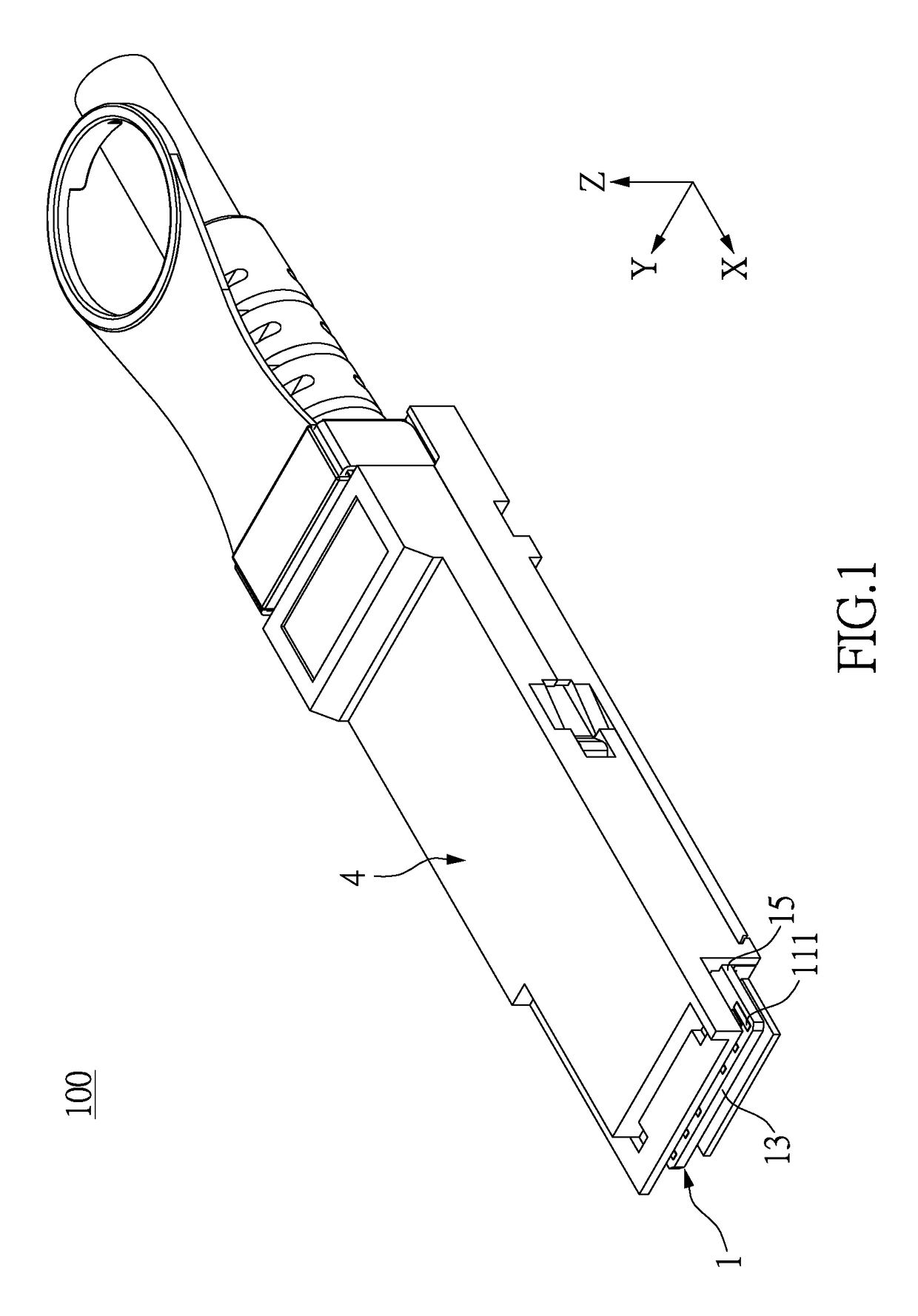
[0027]Please refer to FIGS. 1 through 10, which show a first embodiment of the instant disclosure. References are hereunder made to the detailed descriptions and appended drawings in connection with the instant invention. However, the appended drawings are merely shown for exemplary purposes, rather than being used to restrict the scope of the instant invention.
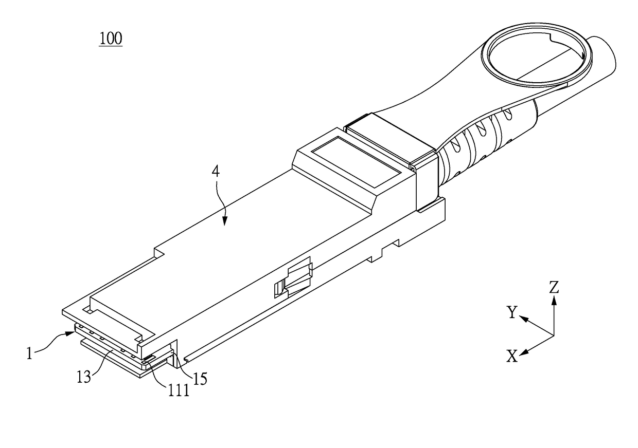
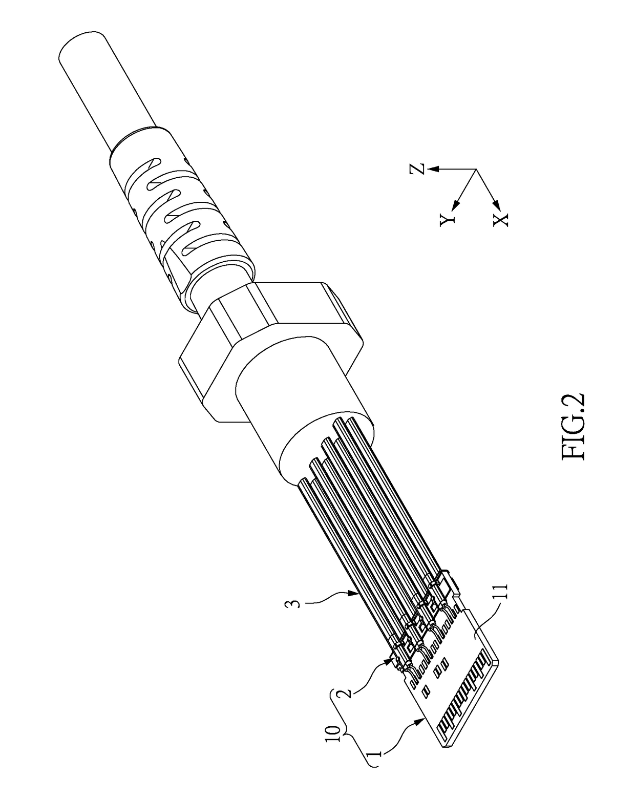
[0028]Please refer to FIGS. 1 through 4, which show a cable connector 100 of the instant embodiment including a circuit board 1, a connecting clip 2, a plurality of conductive cables 3, and a case 4 receiving the circuit board 1, the connecting clip 2, and the conductive cables 3. A front end portion of the circuit board 1 is exposed from the case 4. The conductive cables 3 are positioned on a rear end portion of the circuit board 1 by using the connecting clip 2.
[0029]FIGS. 2 through 10 do not show the case 4 in order to more clearly show the inner construction of the cable connector 100, and each figure sh...
second embodiment
[Second Embodiment]
[0041]Please refer to FIGS. 11 and 12, which show a second embodiment. The second embodiment is similar to the first embodiment, the different features between the two embodiments being the construction of the connecting clip 2 and the corresponding portion of the circuit board 1.
[0042]Specifically, the circuit board 1 is a multi-layer construction and includes a first insulating layer 16, a second insulating layer 17, and a grounding layer 18 arranged between the first insulating layer 16 and the second insulating layer 17. The first surface 11 in the instant embodiment includes an outer surface of the first insulating layer 16, the touching pads 111, and the welding pads 112. The second surface 12 in the instant embodiment includes an outer surface of the second insulating layer 17, the touching pads 121, and the welding pads 122.
[0043]Moreover, at least one hole 113 is inwardly formed on the first surface 11 of the circuit board 1, and the circuit board 1 has a...
third embodiment
[Third Embodiment]
[0047]Please refer to FIGS. 13 and 14, which show a third embodiment. The third embodiment is similar to the first and second embodiments, and the different features of the third embodiment compared to the first and second embodiments are the construction of the connecting clip 2 and the corresponding portion of the circuit board 1.
[0048]Specifically a hole 113′ is inwardly formed on one of the side edges 15 of the circuit board 1 penetrating through the circuit board 1 from the first surface 11 to the second surface 12. The circuit board 1 has a conductive extension 114 coated on an inner wall defining the hole 113′. The connecting clip 2 has a conductive portion 24′ curvedly extended from one of the clamping sheets 212, and the conductive portion 24′ is formed as an elastic arm. The conductive portion 24′ of the connecting clip 2 is inserted into the hole 113′ of the circuit board 1 and abuts against the conductive extension 114 arranged in the hole 113′.
PUM
 Abstract
Description
Claims
Application Information
 - R&D
- Intellectual Property
- Life Sciences
- Materials
- Tech Scout
- Unparalleled Data Quality
- Higher Quality Content
- 60% Fewer Hallucinations
Browse by: Latest US Patents, China's latest patents, Technical Efficacy Thesaurus, Application Domain, Technology Topic, Popular Technical Reports.
© 2025 PatSnap. All rights reserved.Legal|Privacy policy|Modern Slavery Act Transparency Statement|Sitemap|About US| Contact US: help@patsnap.com


