
Image sensor and method of sensing image

a technology which is applied in the field of image sensor and image sensing method, can solve the problems of increasing the noise of fixed pattern, reducing the size of the pixel, and reducing the image quality, so as to reduce or prevent the deterioration of the recognition rate performance, reduce power consumption, and reduce the effect of image quality deterioration

Active Publication Date: 2017-11-28
DONGBU HITEK CO LTD
View PDF3 Cites 0 Cited by
  • Summary
  • Abstract
  • Description
  • Claims
  • Application Information

AI Technical Summary

Benefits of technology

This design effectively cancels column and row noise, improves image quality, and enhances recognition rate performance by accurately correcting active pixel data, while also reducing power consumption based on environmental conditions.

Problems solved by technology

As the number of pixels of an image sensor increases and the size of the image sensor decreases, the size of the pixel decreases and thus influence of dark current, noise generated by the dark current, photon shot noise and / or MOS device noise increases.
The deviation may have a fixed value with respect to each pixel, and may cause fixed pattern noise (FPN) on the image displayed on the screen.
In particular, as the distance between adjacent pixels decreases, an abnormal output image may be generated due to column fixed pattern noise (CFPN) that is generated due to an offset of the pixels or of a processing circuit in one or more (e.g., each) column upon implementing an image.

Method used


Image

  • Image sensor and method of sensing image
  • Image sensor and method of sensing image
  • Image sensor and method of sensing image

Examples


Embodiment Construction

[0040]Hereinafter, embodiments of the present invention will be clearly appreciated through the accompanying drawings and the following description thereof. In description of the embodiments, it will be understood that, when an element such as a layer, film, region, pattern or structure is referred to as being formed “on” or “under” another element, such as a substrate, layer, film, region, pad or pattern, it can be directly “on” or “under” the other element or be indirectly “on” or “under” the other element with intervening elements therebetween. It will also be understood that “on” and “under” the element is described relative to the drawings. In addition, the same reference numerals designate the same constituent elements throughout the description of the drawings.

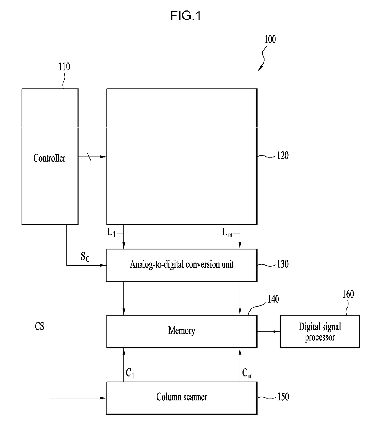
[0041]FIG. 1 is a diagram showing the configuration of an image sensor 100 according to one or more embodiments of the present invention.

[0042]Referring to FIG. 1, the image sensor 100 includes a controller 110, a pixel...


PUM


Abstract

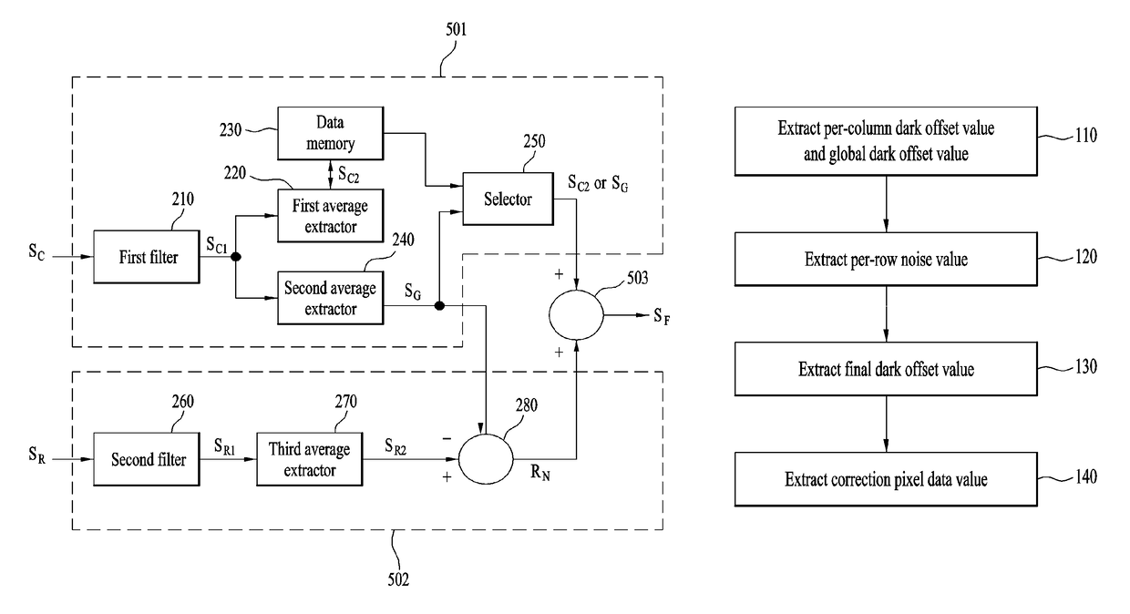
An image sensor includes a pixel array unit including an active pixel area including active pixels, a first dark area including first dark pixels, and a second dark area including second dark pixels, an offset extractor configured to extract a final dark offset value, and a corrector configured to correct pixel data values of the active pixels based on the final dark offset value. The offset extractor extracts a per-column dark offset value, a global dark offset value, a per-row average, and a per-row noise value, selects one of the extracted per-column dark offset value and global dark offset value, and extracts the final dark offset value from the per-row noise value and either the per-column dark offset value or the global dark offset value.

Description

[0001]This application claims the benefit of Korean Patent Application No. 10-2016-0043422, filed on Apr. 8, 2016, which is hereby incorporated by reference as if fully set forth herein.BACKGROUND OF THE INVENTIONField of the Invention[0002]Embodiments of the present invention relate to an image sensor and a method of sensing an image.Discussion of the Related Art[0003]An image sensor is a semiconductor device that converts an optical image into an electrical signal and has been used for a digital camera, a mobile communication terminal, etc. Such an image sensor may include a plurality of unit pixels.[0004]As the number of pixels of an image sensor increases and the size of the image sensor decreases, the size of the pixel decreases and thus influence of dark current, noise generated by the dark current, photon shot noise and / or MOS device noise increases.[0005]In a CMOS type image sensor, characteristics of an active device (for example, a deviation of a threshold voltage Vth) may...

Claims


Application Information

Patent Timeline
Patent Type & Authority Patents(United States)
IPC IPC(8): H04N5/361H04N5/363H04N5/369H04N5/365H04N25/65
CPCH04N5/361H04N5/3696H04N5/3658H04N5/363H04N25/65H04N25/677H04N25/633H04N25/68H04N25/63
Inventor HAN, YONG IN
Owner DONGBU HITEK CO LTD
Learn More