Optical modulation device and driving method thereof

a technology of optical modulation and driving method, which is applied in the direction of optics, static indicating devices, instruments, etc., can solve the problems of difficult uniform alignment process such as rubbing process, display defects may occur, and complicated alignment process including different directions according to the position of the substrate adjacent to the liquid crystal layer, etc., to achieve the effect of reducing manufacturing time, reducing defects due to a pretilt distribution of liquid crystal molecules, and simplifying the manufacturing process of optical modulation devices

Active Publication Date: 2017-11-28
SAMSUNG DISPLAY CO LTD
View PDF8 Cites 0 Cited by
  • Summary
  • Abstract
  • Description
  • Claims
  • Application Information

AI Technical Summary

Benefits of technology

[0009]Exemplary embodiments of the present invention provide an optical modulation device including liquid crystals which may simplify a manufacturing process, reduce manufacturing time, and may reduce or eliminate defects due to the pretilt distribution of liquid crystal molecules.
[0010]Exemplary embodiments of the present invention provide an optical modulation device including liquid crystals, which may reduce or eliminate an occurrence of a texture in the liquid crystal molecules by reinforcing a control force for the liquid crystal molecules and enhancing diffraction efficiency.
[0028]The driving method may include reducing differences between the voltage applied to the upper end of the first lower electrode, the voltage applied to the lower end of the first lower electrode, the voltage applied to the upper end of the second lower electrode, and the voltage applied to the lower end of the second lower electrode, after applying the voltages to the upper end and the lower end of the first lower electrode and the upper end and the lower end of the second lower electrode through the first to fourth channels.
[0031]A manufacturing process of the optical modulation device including the liquid crystals may be simplified and manufacturing time may be reduced. Defects due to a pretilt distribution of liquid crystal molecules may be reduced or eliminated.
[0032]An occurrence of a texture in the liquid crystal molecules may be reduced or eliminated by reinforcing a control force for the liquid crystal molecules to enhance diffraction efficiency.

Problems solved by technology

An aligning process including different directions according to positions of the substrate adjacent to the liquid crystal layer may be relatively complicated.
When the aligning process includes minutely divided regions, it may be difficult to uniformly perform the aligning process such as a rubbing process.
When the aligning process is used in the display device, display defects may occur.

Method used


Image

  • Optical modulation device and driving method thereof
  • Optical modulation device and driving method thereof
  • Optical modulation device and driving method thereof

Examples


Embodiment Construction

[0046]Exemplary embodiments of the present invention will be described more fully hereinafter with reference to the accompanying drawings. Exemplary embodiments of the present invention may be embodied in different forms and should not be construed as limited to the exemplary embodiments set forth herein.

[0047]In the drawings, the thickness of layers, films, panels, or regions may be exaggerated for clarity. Like reference numerals may refer to like elements throughout the specification and drawings. It will be understood that when an element such as a layer, film, region, or substrate is referred to as being “on” another element, it may be directly on the other element or intervening elements may be present.

[0048]An optical modulation device according to an exemplary embodiment of the present invention will be described below in more detail with reference to FIGS. 1 to 3.

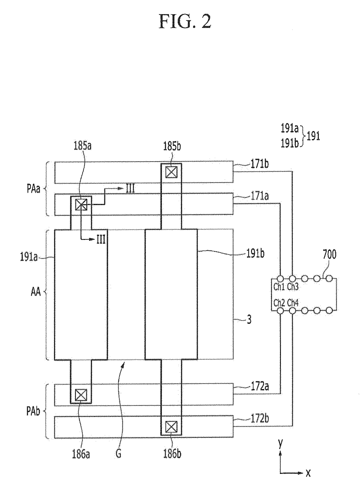
[0049]FIG. 1 is a perspective view of an optical modulation device according to an exemplary embodiment of the p...


PUM

PropertyMeasurementUnit
voltageaaaaaaaaaa
azimuthal anglesaaaaaaaaaa

Abstract

Provided are an optical modulation device and a driving method thereof. The optical modulation device includes an active area and a peripheral area disposed around the active area. A plurality of lower electrodes is disposed in the active area. The plurality of lower electrodes extends in a first direction. The plurality of lower electrodes includes a first lower electrode and a second lower electrode. A driver is configured to apply a driving signal to the first lower electrode and the second lower electrode. The driver includes a first channel connected with an upper end of the first lower electrode, a second channel connected with a lower end of the first lower electrode, a third channel connected with an upper end of the second lower electrode, and a fourth channel connected with a lower end of the second lower electrode.

Description

CROSS-REFERENCE TO RELATED APPLICATION[0001]This application claims priority under 35 U.S.C. §119 to Korean Patent Application No. 10-2014-0172361 filed in the Korean Intellectual Property Office on Dec. 3, 2014, the disclosure of which is incorporated by reference herein in its entirety.TECHNICAL FIELD[0002]Exemplary embodiments of the present invention relate to an optical modulation device and more particularly to a driving method for the optical modulation device.DISCUSSION OF RELATED ART[0003]Optical devices may include an optical modulation device that modulates a characteristic of light. For example, an optical display device may display a 3D image. An optical modulation device for dividing and transmitting an image at different viewpoints may display a 3D image. An optical modulation device may be used in an autostereoscopic 3D image display device, and may include a lens and a prism, which may change a path of light of an image in the display device to transmit the light to...

Claims


Application Information

Patent Timeline
Patent Type & Authority Patents(United States)
IPC IPC(8): G02F1/133G02F1/29G02F1/13363G02F1/1343G02F1/139
CPCG02F1/13306G02F1/13363G02F1/29G02F2203/62G02F1/134363G02F2001/133631G02F2001/294G02F1/1393G02F1/133631G02F1/294G02B26/06Y10S359/903
Inventor JEONG, SEUNG JUNSEO, HYUN SEUNGCHO, JUNG-HYUN
Owner SAMSUNG DISPLAY CO LTD
Why Eureka
Try Eureka