Switching element driving circuit

a driving circuit and switching element technology, applied in the direction of pulse technique, multiple input and output pulse circuits, power conversion systems, etc., can solve the problems of long delay time, difficult high-speed response, easy influence of control response time via differential amplifier amps, etc., to improve control responsiveness, good control responsiveness, and gate voltage

Active Publication Date: 2017-08-29
FUJI ELECTRIC CO LTD
View PDF10 Cites 4 Cited by
  • Summary
  • Abstract
  • Description
  • Claims
  • Application Information

AI Technical Summary

Benefits of technology

[0013]With the foregoing in view, it is an object of the present invention to provide a switching element driving circuit that has fast control responsiveness to the gate voltage of the switching element when the overcurrent is detected, and can effectively protect the switching element from the overcurrent by quickly converging the gate voltage to a predetermined voltage.
[0017]According to the switching element driving circuit having the above configuration, if the output voltage of the driving circuit main unit exceeds the first reference voltage, the first control element connected to the control terminal of the switching element is turned ON by the comparator, and the gate voltage of the switching element is quickly dropped. Furthermore, this control is performed simply by driving the first control element ON, hence, compared with the conventional feedback control of the gate voltage via the differential amplifier, the gate voltage of the switching element can be more quickly dropped and the control responsiveness can be improved.
[0018]Moreover, the feedback control of the second control element by the differential amplifier is activated after the control to drop the gate voltage by the comparator, based on the difference of control responsiveness, is activated. As a result, the gate voltage is controlled via the second control element, under control of the differential amplifier, and the gate voltage converges to a predetermined voltage. Therefore when overcurrent is generated, the gate voltage is quickly converted to a predetermined voltage with good control responsiveness, by a combination of the control of the first control element using the comparator and the control of the second control element using the differential amplifier, and this converted state can be stably held. As a consequence, the responsiveness when the overcurrent is generated can be increased, and the switching element can be protected with certainty.

Problems solved by technology

However in the case of the above mentioned feedback control loop via the differential amplifier AMP, delay time is long.
This means that high-speed response is difficult when overcurrent is detected.
Another problem is that the control response time via the differential amplifier AMP is easily influenced by the gate capacitance of the switching element Q2.

Method used


Image

  • Switching element driving circuit
  • Switching element driving circuit
  • Switching element driving circuit

Examples


Embodiment Construction

[0026]A switching element driving circuit according to an embodiment of the present invention will now be described with reference to the drawings.

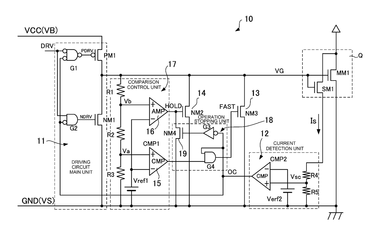
[0027]FIG. 1 is a schematic block diagram depicting a key section of the switching element driving circuit 10 according to the embodiment, where Q is a switching element driven by the switching element driving circuit 10. This switching element Q is constituted by an n-channel high voltage MOS-FET (MM1), for example, and includes a MOS-FET (SM1) for current detection which is connected in parallel. The MOS-FET for current correction (SM1) includes a channel region that is [1 / n] of the high voltage MOS-FET (MM1), and outputs [1 / 100] current Is, for example, that is in proportion to the current flowing through the high voltage MOS-FET (MM1).

[0028]The switching element driving circuit 10 is configured so as to operate by receiving power supply voltage VCC, of which reference potential is the ground potential (GND), for example. To drive the ...


PUM


Abstract

A switching element driving circuit includes a current detection unit that outputs a driving stop signal based on a level of current flowing through the switching element, and first and second control elements each connected to a control terminal of the switching element. A comparator controls the first control element based on a result of comparison of an output voltage of the driving circuit main unit with a first reference voltage. A differential amplifier drives the second control element in accordance with a voltage difference between the output voltage of the driving circuit main unit and a second reference so as to maintain the output voltage equal to the second reference voltage. An operation stopping unit stops the comparator and the differential amplifier to drive the first and second control elements, respectively, in response to the driving stop signal.

Description

CROSS-REFERENCE TO RELATED APPLICATION[0001]This is a continuation application of International Application number PCT / JP2014 / 058536, which was filed on Mar. 26, 2014 and designated the United States. Furthermore, this application claims the benefit of foreign priority of Japanese application number 2013-087316, filed on Apr. 18, 2013. The disclosures of both of these earlier applications are incorporated herein by reference.BACKGROUND OF THE INVENTION[0002]Technical Field[0003]The present invention relates to a switching element driving circuit that includes an overcurrent protection function for such switching elements as IGBT (insulated-gate bipolar transistor) and MOS-FET (metal-oxide-semiconductor field-effect transistor).[0004]Background Art[0005]A well-known power converter to drive AC load is a power converter having two switching elements Q1 and Q2, which are totem pole-connected to form a half bridge circuit, and alternately turn ON / OFF so as to switch the DC voltage. The ...

Claims


Application Information

Patent Timeline
Patent Type & Authority Patents(United States)
IPC IPC(8): H02H3/00H03K5/24H03K17/082H03K17/16H02H3/08H02H7/12H03K17/687H02M1/00
CPCH03K17/082H02H3/08H02H7/12H03K5/24H03K17/0828H03K17/168H03K17/6871
Inventor AKAHANE, MASASHI
Owner FUJI ELECTRIC CO LTD
Why Eureka
Try Eureka