Method for preparing a semiconducting layer

a semiconducting layer and semiconducting technology, applied in semiconductor devices, solid-state devices, electrical apparatus, etc., can solve the problems of difficult to obtain repeatable results from solutions, limiting the performance of small molecule semiconductors in otfts, film roughness, etc., to reduce contact resistance, reduce vertical crystal growth, and improve homogeneity

Active Publication Date: 2017-04-11
CAMBRIDGE DISPLAY TECH LTD
View PDF9 Cites 0 Cited by
  • Summary
  • Abstract
  • Description
  • Claims
  • Application Information

AI Technical Summary

Benefits of technology

[0054]Preferably heating is carried out immediately after deposition, i.e. without any intervening steps. As explained below in more detail, the evaporation of solvent during the deposition step is suppressed and the required wet film thickness of semiconducting layer is achieved without any solvent loss. When followed by a heating step, especially a rapid heating step, this enables a semiconducting layer having a homogeneous lateral distribution of non-polymeric semiconductor in a matrix of polymeric semiconductor to be formed.
[0171]The improved lateral distribution of non-polymeric semiconductor in the semiconducting layer manifests itself in reduced contact resistance, particularly for short channel length devices (<20 μm). In short channel length devices contact resistance can contribute a significant proportion to the total channel resistance in the device. The higher the contact resistance in the device, the higher the proportion of the applied voltage is dropped across the source and drain contacts and, as a result, the lower the bias across the channel region is achieved. A high contact resistance has the effect of a much lower current level being extracted from the device due to the lower bias applied across the channel region, and hence lower device mobility.

Problems solved by technology

Unfortunately, however, it can be difficult to obtain repeatable results from solution processed films of small molecule semiconductors and this is believed to be due to their poor film forming properties.
Issues with material reticulation from and adhesion to substrates, film roughness and film thickness variations can limit the performance of small molecule semiconductors in OTFTs.
Film roughness can be a further problem for top gate organic thin film transistors as the accumulation layer is formed at the uppermost surface of the semiconducting layer.

Method used


Image

  • Method for preparing a semiconducting layer
  • Method for preparing a semiconducting layer
  • Method for preparing a semiconducting layer

Examples


example 1

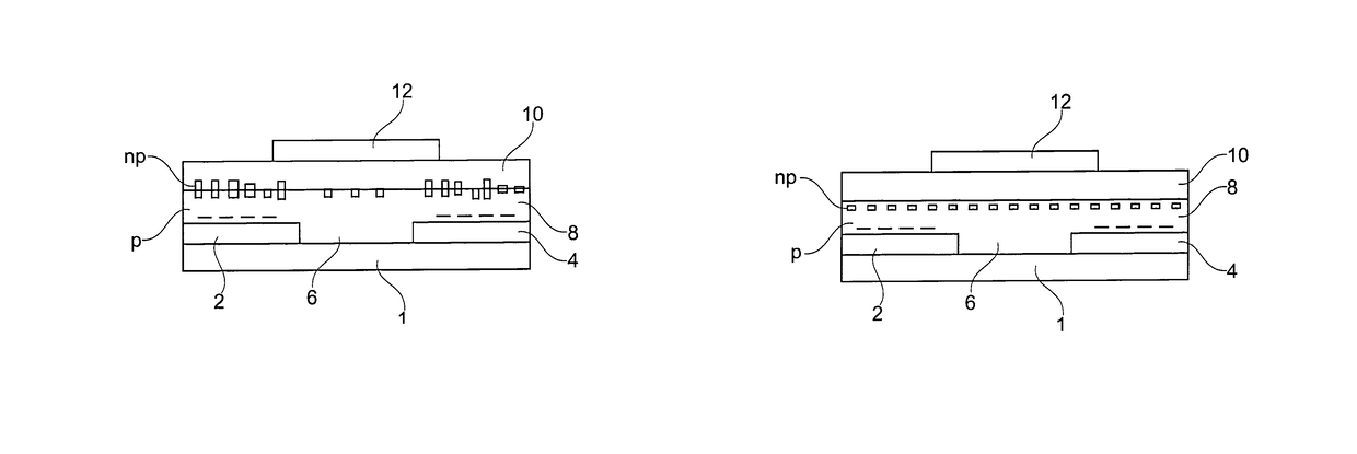
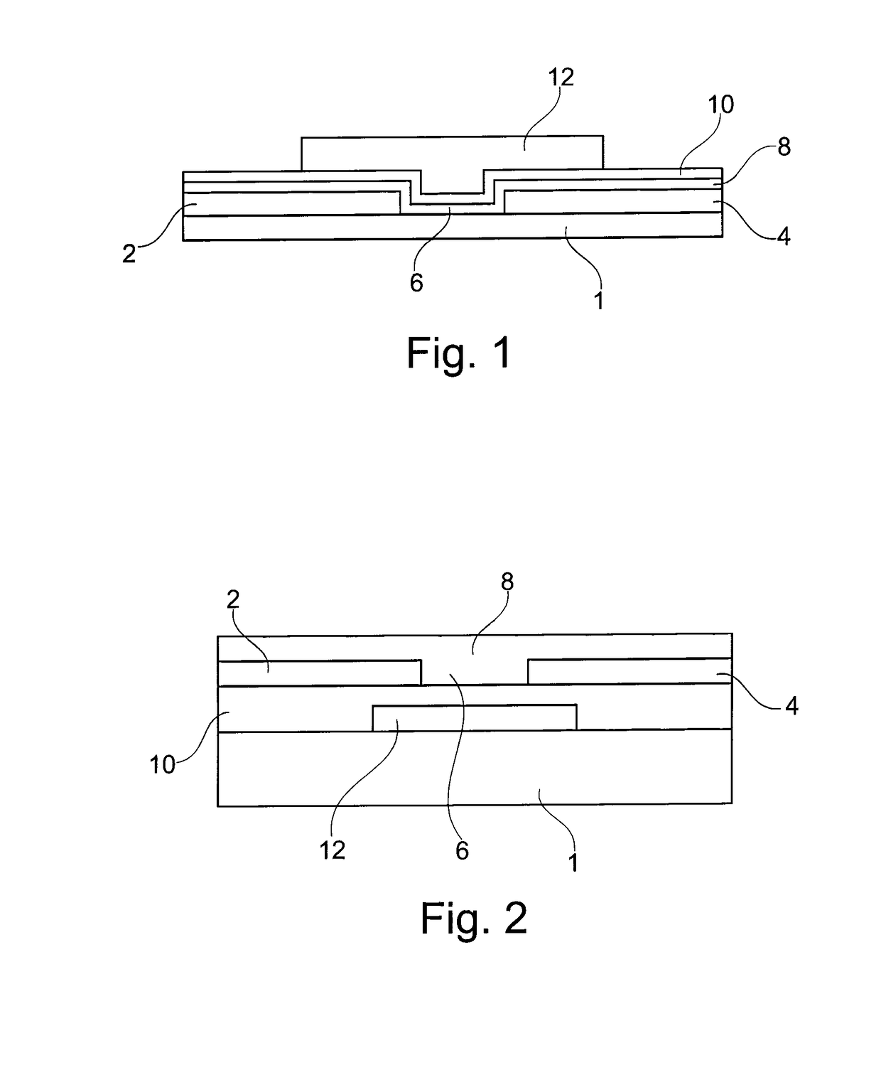
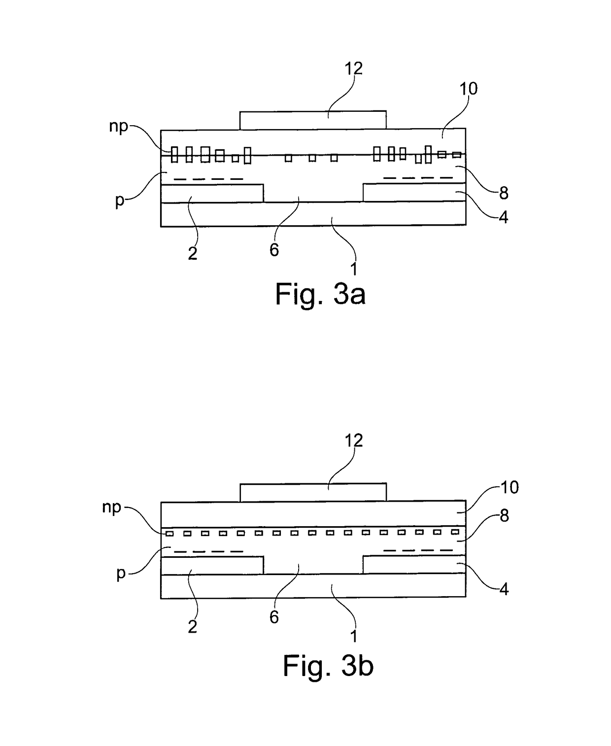
[0204]In this first example, atomic force microscopy images were taken of devices prepared as described in the above preparative example with a semiconducting layer deposited from either o-xylene alone (as a comparative example) or from solvent mixtures comprising o-xylene and one of either 2-methylanisole, 1,3-dimethoxybenzene or ethylbenzoate.

[0205]The use of o-xylene alone results in solvent evaporation taking place during the deposition of the semiconducting layer. This results in a device in which isolated domains of the non-polymeric semiconductor embedded in the polymer matrix, as can be seen in FIG. 4a (top figure). The 3D AFM (height data) analysis highlights that the channel region of the device mostly comprises the polymeric semiconductor (FIG. 4a, bottom figure), leading to a low mobility device.

[0206]In comparison, it can be seen in FIGS. 4b, 4c and 4d that in devices in which the semiconducting layer was deposited from a solution of o-xylene and one other higher boilin...

example 2

[0207]Mobility data for devices with semiconducting layers deposited from either o-xylene alone or from o-xylene with a higher boiling solvent is shown in FIG. 5. Average peak mobility (in cm2 / Vs) was measured at a range of channel lengths used in the test cells (5 to 100 μm). Devices with the shortest channel lengths were generally found to exhibit lower mobilities (contact resistance is the more dominant component compared to the total channel resistance) and vice versa.

[0208]The use of o-xylene in combination with a second higher boiling point aromatic solvent (in these examples, 2-methylanisole, tetralin, ethylbenzoate and 1,3-dimethoxybenzene) very clearly highlights the improvement in device performance, with those devices exhibiting mobilities of upwards of around 0.2 to 0.8 cm2 / Vs for all channel lengths tested. In comparison, in the device in which o-xylene alone was used, mobilities of between 0.1 and 0.3 cm2 / Vs were measured, with a mobility of greater than 0.2 cm2 / Vs onl...


PUM

PropertyMeasurementUnit
boiling pointaaaaaaaaaa
polydispersityaaaaaaaaaa

Abstract

A method for preparing a semiconducting layer of an organic electronic device comprising: (i) depositing said semiconducting layer from a solution comprising a polymeric semiconductor, a non-polymeric semiconductor, a first aromatic solvent and a second aromatic solvent, wherein said second aromatic solvent has a boiling point that is at least 15° C. higher than the boiling point of said first aromatic solvent; and (ii) heating said deposited layer to evaporate said solvent, wherein said first aromatic solvent is of formula (I): wherein R1 is selected from C1-6 alkyl and OC1-6 alkyl; and R2 and R3 are each independently selected from H and CC1-6 alkyl.

Description

RELATED APPLICATIONS[0001]The present application is a national stage filing under 35 U.S.C. §371 of international PCT application, PCT / GB2013 / 000267, filed Jun. 17, 2013, which claims priority to United Kingdom patent application, GB 1210858.5, filed Jun. 19, 2012, each of which is incorporated herein by reference.FIELD OF THE INVENTION[0002]The present invention relates to a method for preparing a semiconducting layer of an organic electronic device and in particular to a method of preparing a thin film transistor comprising a semiconducting layer prepared by the method. The invention is also concerned with blends for preparing the semiconducting layer and with organic electronic devices comprising a semiconducting layer prepared by the methods of the invention.BACKGROUND[0003]Transistors may be formed by processes wherein their semiconducting layer, and in many cases, other layers is deposited from solution. The resulting transistors are called thin-film transistors. When an orga...

Claims


Application Information

Patent Timeline
Patent Type & Authority Patents(United States)
IPC IPC(8): H01L51/00H01L51/05H01L21/02
CPCH01L51/0039H01L21/02118H01L51/0007H01L51/0035H01L51/0074H01L51/0566H01L51/0026H01L51/0043H01L51/0512H10K71/15H10K85/115H10K85/151H10K85/6576H10K10/462H10K10/488H10K10/486H10K50/00H10K85/111H10K71/40
Inventor NEWSOME, CHRISTOPHER
Owner CAMBRIDGE DISPLAY TECH LTD
Why Eureka
Try Eureka