Semiconductor system for implementing an ising model of interaction

a technology of ising model and system, applied in the field of ising model implementation of ising model, can solve the problems of not easy to extract parallelism from a program created, acquisition of ground state of ising model in which a topology has a non-plane graph is a np-hard problem, and the difficulty of neumann-type computers in view of computation tim

Active Publication Date: 2017-03-07
HITACHI LTD
View PDF3 Cites 3 Cited by
  • Summary
  • Abstract
  • Description
  • Claims
  • Application Information

AI Technical Summary

Benefits of technology

[0017]In a semiconductor device for calculating the interaction model, the typical effect can provide a technique capable of executing interaction calculation in non-synchronization with a clock.

Problems solved by technology

However, it is not easy to extract the parallelism from a program created by writing down the sequential algorithm as the instruction string.
However, inter-planet influence is not limited between two planets, and three or more planets affect each other, and exhibit complicated behaviors (which becomes a problem referred to as so-called three-body problem and many-body problem).
It is known that acquirement of a ground state of the Ising model in which a topology has a non-plane graph is an NP-hard problem.
Incidentally, since the acquirement of the ground state of the Ising model is the NP-hard problem as described above, the solution by the Neumann-type computer is accompanied by a difficulty in view of computation time.

Method used


Image

  • Semiconductor system for implementing an ising model of interaction
  • Semiconductor system for implementing an ising model of interaction
  • Semiconductor system for implementing an ising model of interaction

Examples


embodiment

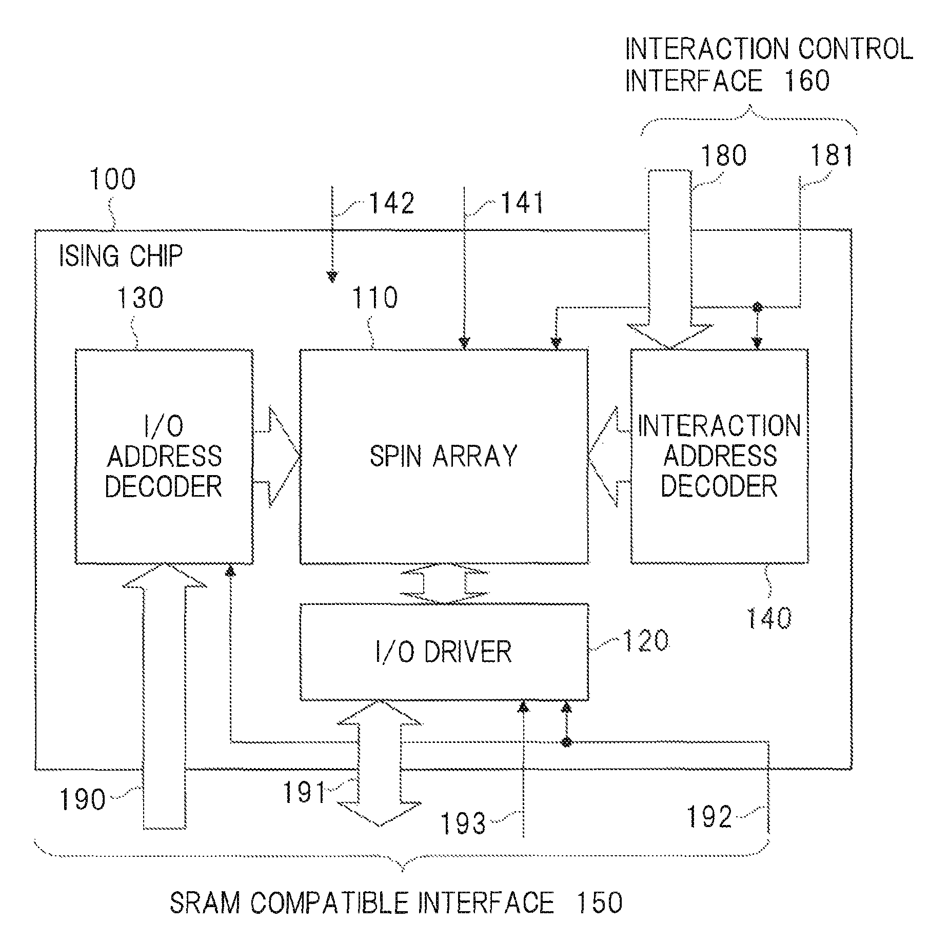
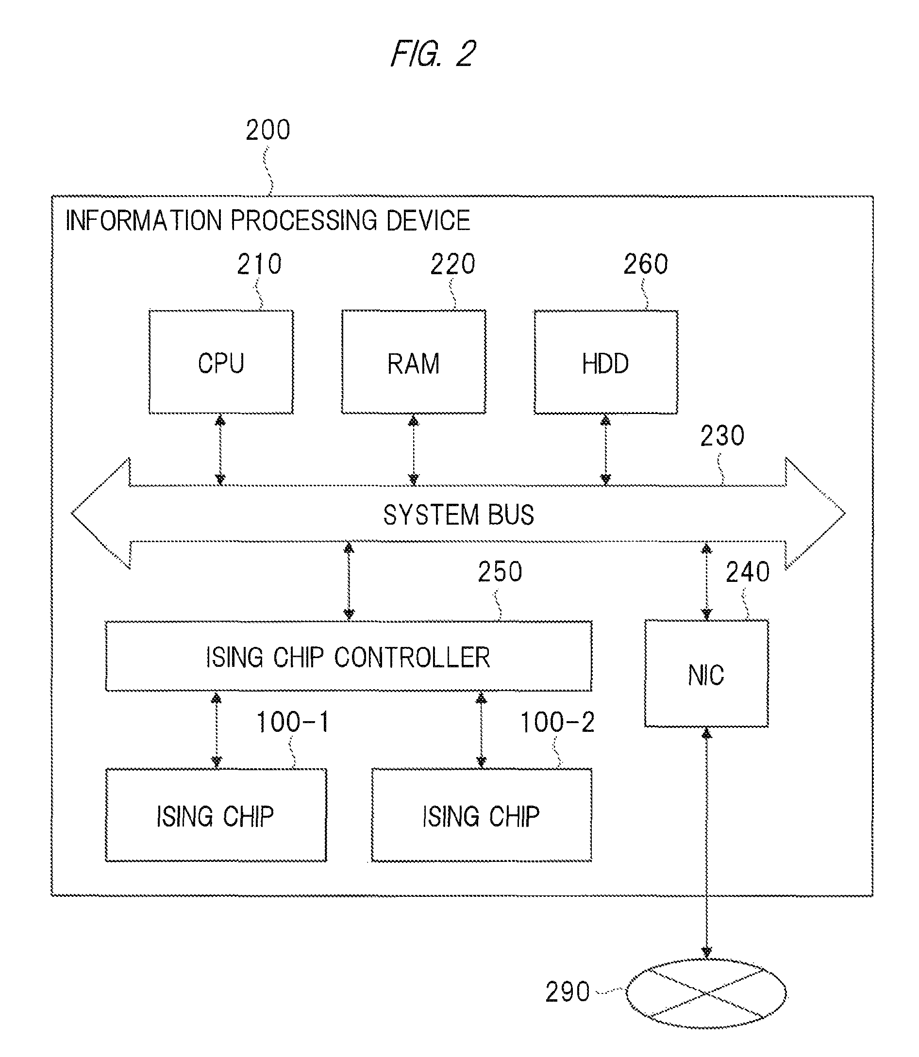
[0035]The present embodiment relates to a semiconductor device which calculates an interaction model, and relates to an information processing device which controls the semiconductor device as an accelerator.

0. Definition of Interaction Model

[0036]Various physical phenomena and social phenomena can be expressed by an interaction model. The interaction model is a model defined by a plurality of nodes forming the model, an interaction among the nodes, and besides, a bias for every node as needed. While various models are proposed in physics or social sciences, all of them can be interpreted as one aspect of the interaction model. In addition, as a feature of the interaction model, an influence among the nodes is limited to an interaction between two nodes (interaction between two bodies). For example, when dynamics of planets in cosmic space is considered, this case can be interpreted also as one type of the interaction model in a point that an interaction caused by universal gravity ...


PUM


Abstract

In a semiconductor device which calculates an interaction model, a technique capable of executing interaction calculation in non-synchronization with a clock is provided. The semiconductor device includes a plurality of units each of which includes: a first memory cell for storing a value indicating a state of one node of an interaction model; a second memory cell for storing an interaction coefficient indicating an interaction from a node connected to the one node; and an interaction calculation circuit for determining a value indicating a next state of the one node based on a current determined by a value indicating a state of the connected node and the interaction coefficient.

Description

CROSS-REFERENCE TO RELATED APPLICATION[0001]The present application claims priority from Japanese Patent Application No. 2014-176385 filed on Aug. 29, 2014, the content of which is hereby incorporated by reference into this application.TECHNICAL FIELD OF THE INVENTION[0002]The present invention relates to a semiconductor device. More particularly, the present invention relates to a semiconductor device to calculate an interaction model, and relates to an information processing device to control the semiconductor device as an accelerator.BACKGROUND OF THE INVENTION[0003]Currently, a mainstream of a computer architecture is a Neumann type. An operation of the Neumann-type architecture is defined by a program which is a sequential instruction string. The Neumann-type architecture has such general versatility as being available for various uses by changing the program. Not only a CPU (Central Processing Unit) that plays a central role of a computer but also a specific-use arithmetic dev...

Claims


Application Information

Patent Timeline
Patent Type & Authority Patents(United States)
IPC IPC(8): G06F13/16G11C7/10G11C5/08G11C14/00G11C11/16G06N7/00G06N99/00
CPCG06F13/1668G06F13/1652G06N7/005G11C5/08G11C7/1006G11C11/16G11C14/0081G06N99/002G11C2213/71G06N10/00G06N7/01
Inventor YAMAOKA, MASANAOOSHIMA, TAKASHIHAYASHI, MASATO
Owner HITACHI LTD
Why Eureka
Try Eureka