Electronic device, electronic apparatus, and method of manufacturing electronic device
a technology of electronic equipment and electronic components, applied in the field of electronic equipment and electronic equipment manufacturing, can solve the problems of significantly affecting the yield ratio, dramatic deformation of the yield ratio, and degradation of the reliability of the functional element, so as to achieve the effect of reducing the size and space of the devi
- Summary
- Abstract
- Description
- Claims
- Application Information
AI Technical Summary
Benefits of technology
Problems solved by technology
Method used
Image

Examples
first embodiment
1.1. First Embodiment
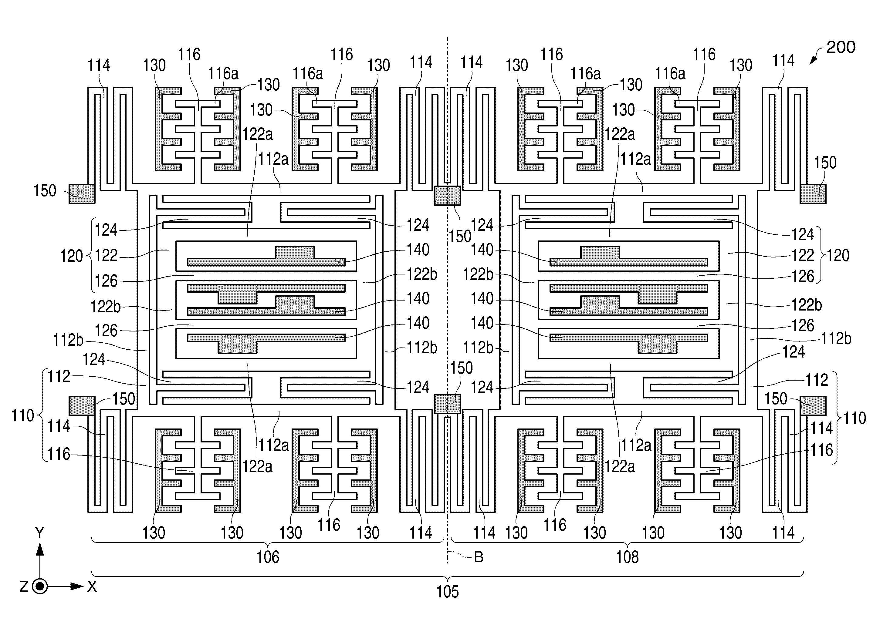
[0070]Firstly, an electronic device according to a first embodiment will be explained with reference to the accompanying drawings. FIG. 1 is a cross-sectional view schematically showing an electronic device 100 according to the first embodiment. For the sake of convenience, in the drawing, the X axis, the Y axis, and the Z axis are shown as the three axes perpendicular to each other.
[0071]As shown in FIG. 1, the electronic device 100 includes a first cavity 41 composed of a first base body 10, a second base body 20, and a third base body 30, a package 40 having a second cavity 42, and first and second functional elements 200, 300 housed in the package 40. It should be noted that, for the sake of convenience, the first and second functional elements 200, 300 are simplified in FIG. 1.
[0072]The electronic device 100 is a composite element sensor having a plurality of physical quantity detection sensors mounted in the same package (the same substrate). The first and...
first modified example
[0141]Then, a first modified example of the first embodiment will be explained with reference to FIG. 8. FIG. 8 is a cross-sectional view schematically showing an electronic device 101 according to the first modified example. The electronic device 101 according to the first modified example is different from the electronic device 100 according to the first embodiment in the shapes of the first base body 10, the second base body 20, and the third base body 30. In the following description, only the points in which the electronic device 101 is different from the electronic device 100 according to the first embodiment will be explained. The members having already been explained will be denoted with the same reference symbols, and the detailed explanation thereof will be omitted.
[0142]As shown in the drawing, in the electronic device 101 according to the first modified example, the third base body 30 is not provided with the first recessed section 33 and the second recessed section 34, ...
second modified example
[0146]Then, a second modified example of the first embodiment will be explained with reference to FIG. 9. FIG. 9 is a cross-sectional view schematically showing an electronic device 102 according to the second modified example. The electronic device 102 according to the second modified example is different from the electronic device 100 according to the first embodiment in the shape of a third base body 330. In the following description, only the points in which the electronic device 102 is different from the electronic device 100 according to the first embodiment will be explained. The members having already been explained will be denoted with the same reference symbols, and the detailed explanation thereof will be omitted.
[0147]As shown in the drawing, in the electronic device 102 according to the second modified example, the third base body 330 is not provided with the first recessed section 33 and the second recessed section 34, but is provided with an opening section 331 for co...
PUM
| Property | Measurement | Unit |
|---|---|---|
| angular velocity | aaaaa | aaaaa |
| pressure | aaaaa | aaaaa |
| physical quantity | aaaaa | aaaaa |
Abstract
Description
Claims
Application Information
 - R&D
- Intellectual Property
- Life Sciences
- Materials
- Tech Scout
- Unparalleled Data Quality
- Higher Quality Content
- 60% Fewer Hallucinations
Browse by: Latest US Patents, China's latest patents, Technical Efficacy Thesaurus, Application Domain, Technology Topic, Popular Technical Reports.
© 2025 PatSnap. All rights reserved.Legal|Privacy policy|Modern Slavery Act Transparency Statement|Sitemap|About US| Contact US: help@patsnap.com