Touch screen panel and method for manufacturing the same, and display device

a technology of touch screen panel and manufacturing method, applied in the field of touch technologies, can solve the problems of lowering production efficiency and increasing production cost, and achieve the effects of reducing production cost, reducing patterning times during the manufacturing process, and improving manufacturing efficiency of touch screen panel

Active Publication Date: 2016-08-30
BOE TECH GRP CO LTD
View PDF20 Cites 0 Cited by
  • Summary
  • Abstract
  • Description
  • Claims
  • Application Information

AI Technical Summary

Benefits of technology

[0006]The embodiments of the invention provide a method for manufacturing a touch screen panel, which solves the problem of the prior art that the number of times the masks are used is large during the manufacturing of an OGS touch module and the production efficiency is low. Moreover, the embodiments of the invention further provide a touch screen panel with a novel structure that is prepared by the method according to the invention, and a display device containing the touch screen panel.
[0015]The above embodiments of the invention have the following beneficial effects:
[0016]The embodiments of the invention provide a touch screen panel and a method for manufacturing the same, and a display device. The method comprises: forming a pattern of a touch electrode layer on a substrate; forming a pattern of an insulating layer on the touch electrode layer; and then forming the patterns of a bridging layer and a peripheral wiring on the insulating layer by one patterning process. In the invention, the patterning of the bridging layer and the peripheral wiring is accomplished simultaneously in one patterning process, thus the number of patterning times during the manufacture process can be reduced, the manufacture efficiency of the touch screen panel can be improved, and the production cost can be lowered. Moreover, the embodiments of the invention further provide a touch screen panel with a novel structure that is prepared by the method according to the invention and a display device containing the touch screen panel.

Problems solved by technology

In the above preparing process, the number of masks used is large, and each mask is required to be accurately aligned with the substrate when it is used, thus the production efficiency is lowered and the production cost is increased.

Method used


Image

  • Touch screen panel and method for manufacturing the same, and display device
  • Touch screen panel and method for manufacturing the same, and display device
  • Touch screen panel and method for manufacturing the same, and display device

Examples


Embodiment Construction

[0026]The specific embodiments of a touch screen panel and a method for manufacturing the same, and a display device according to the embodiments of the invention will be illustrated in detail below in conjunction with the drawings.

[0027]In the drawings, the thickness of each layer of thin film and the size and shape of each region do not reflect the real proportion; instead, they are only used for schematically illustrating the contents of the invention.

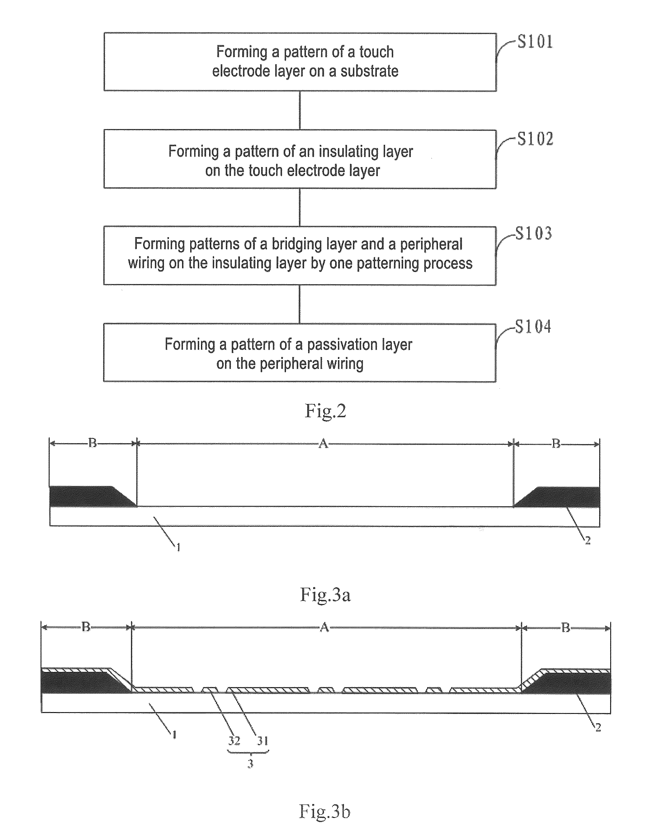
[0028]According to one embodiment of the invention, there provides a method for manufacturing a touch screen panel, as shown in FIG. 2, which specifically includes the steps of:

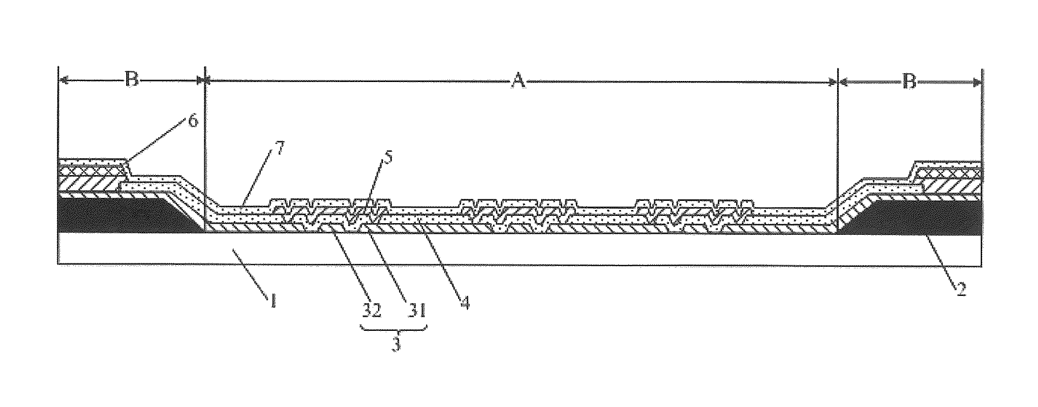
[0029]Step S101: forming a pattern of a touch electrode layer 3 on a substrate 1, wherein the touch electrode layer 3 includes a touch sensing electrode 31 and a touch driving electrode 32 that are formed crosswise and insulated from each other, and as shown in FIG. 3b, the touch electrode layer 3 has a pattern in both a touch region A and a non-touch region ...


PUM

PropertyMeasurementUnit
photosensitiveaaaaaaaaaa
transparentaaaaaaaaaa
transparent conductiveaaaaaaaaaa

Abstract

The present invention discloses a touch Screen panel and a method for manufacturing the same, and a display device. The method comprises: forming a pattern of a touch electrode layer on a substrate; forming a pattern of an insulating layer on the touch electrode layer; and then forming the patterns of a bridging layer and a peripheral wiring on the insulating layer by one patterning process. In the invention, the patterning of the bridging layer and the peripheral wiring is accomplished simultaneously in one patterning process, thereby the number of patterning times during the manufacture process can be reduced, the manufacture efficiency of the touch screen panel can be improved, and the production cost can be lowered.

Description

CROSS REFERENCE TO RELATED APPLICATION[0001]This application is the U.S. national phase of PCT Application No. PCT / CN2013 / 089594 filed on Dec. 17, 2013, which claims priority to Chinese Patent Application No. 201310390465.8 filed on Aug. 30, 2013, the disclosures of which are incorporated in their entirety by reference herein.FIELD OF THE INVENTION[0002]The present invention relates to the field of touch technologies, and in particular, to a touch screen panel and a method for manufacturing the same, and a display device.DESCRIPTION OF THE PRIOR ART[0003]With the rapid development of display technologies, touch screen panel has been gradually popularized in people's life. At present, the touch screen panel may be divided according to its operating principle into resistive touch screen panel, capacitive touch screen panel, infrared touch screen panel, surface acoustic wave touch screen panel, electromagnetic touch screen panel, vibration wave sensitive touch screen panel and inhibite...

Claims


Application Information

Patent Timeline
Patent Type & Authority Patents(United States)
IPC IPC(8): G06F3/047G06F3/044
CPCG06F3/044G06F2203/04103G06F2203/04111Y10T29/49155G06F3/0443G06F3/0446
Inventor HAO, GUANGYEIM, YUNSIK
Owner BOE TECH GRP CO LTD
Why Eureka
Try Eureka