Method for manufacturing a composite compensating balance spring
a technology of compensating balance and composite materials, which is applied in the direction of frequency stabilisation mechanisms, instruments, horology, etc., can solve the problems of difficult to secure to each other and thus produce, and achieve the effect of a wide range of materials
- Summary
- Abstract
- Description
- Claims
- Application Information
AI Technical Summary
Benefits of technology
Problems solved by technology
Method used
Image

Examples
first embodiment
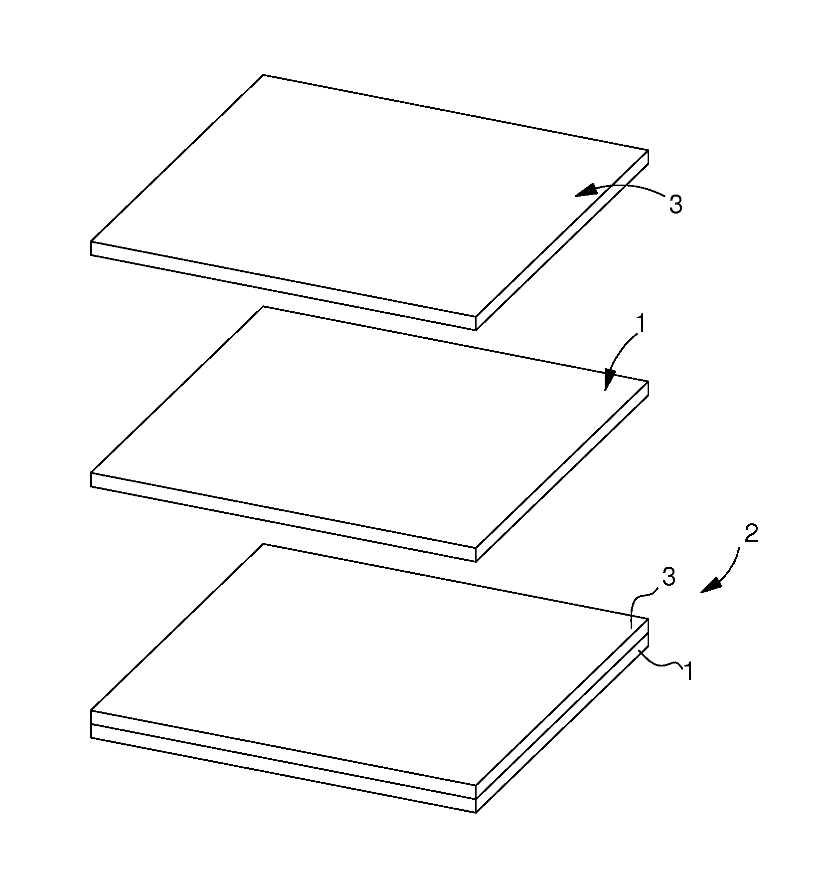
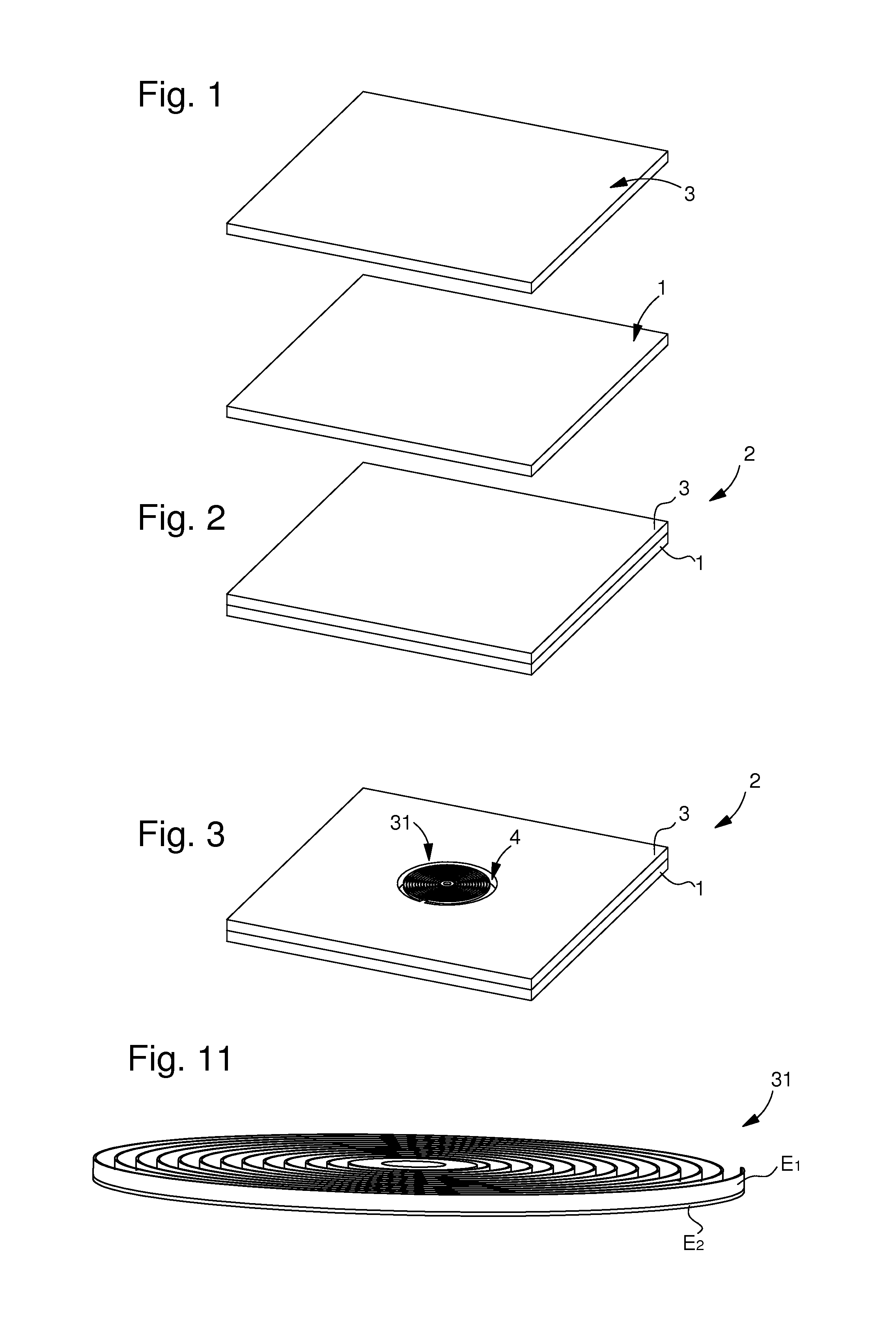
[0053]According to the invention illustrated in FIGS. 1 to 3, the manufacturing method includes a first step a) intended to take a first wafer 1 made of a first material. A second step b) is intended to take at least a second wafer 3 made of at least a second material whose Young's modulus variations with temperature (TEC) are of the opposite sign to those (TEC) of the first material.
[0054]As seen in FIG. 2, a third step c) is intended to join or bond the first wafer 1 to said at least one second wafer 3 in order to form a substrate 2. Depending on the materials used, there are several possible bonding methods. In a non-limiting manner, one may mention the direct welding of surfaces by electromagnetic radiation using a laser, as, for example, explained in EP Patent No 1436830, which is incorporated by reference in this description. It is also perfectly possible to envisage using anodic bonding, fusion bonding, thermocompression bonding, reflow bonding, eutectic bonding, ultrasonic b...
second embodiment
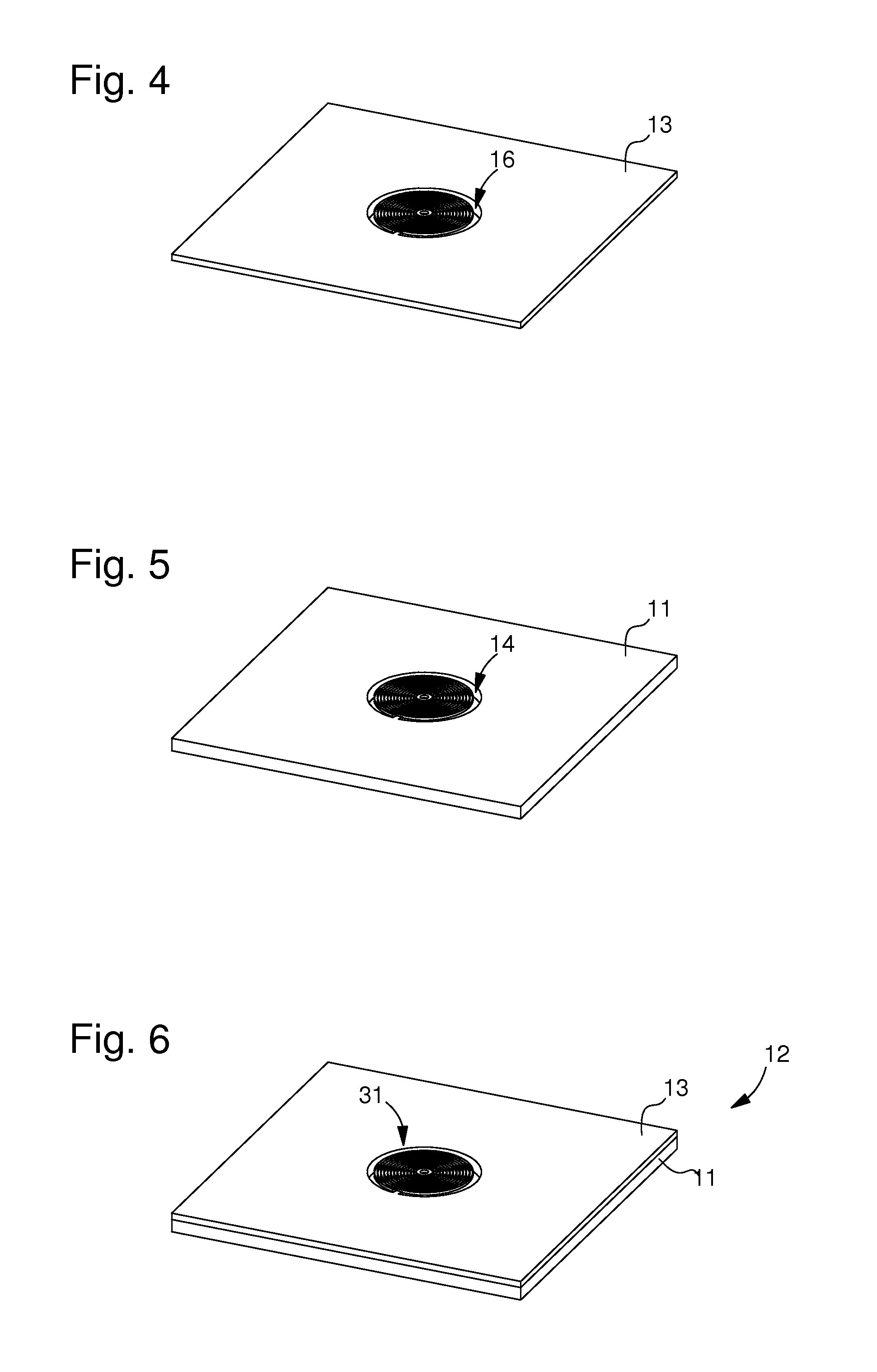
[0057]According to the invention illustrated in FIGS. 4 to 6, the manufacturing method includes a first step a) intended to take a first wafer 11 of a first material. A second step b) is intended to take at least a second wafer 13 made of at least a second material whose Young's modulus variations with temperature (TEC) are of the opposite sign to those (TEC) of the first material.
[0058]As seen in FIGS. 4 and 5, a third step d′) is intended to etch identical patterns 14, 16 through each of wafers 11, 13. Depending on the materials used, there are several possible etches. In a non-limiting manner, a dry etching such as a deep reactive ionic etching (DRIE), laser etching or a plasma etching may be mentioned. It is also perfectly possible to envisage using a wet etching, such as a chemical etching. Finally, it is also possible to perform photostructuration mixing photolithography of a resin followed by a dry etching or wet etching.
[0059]The method according to the second embodiment con...
third embodiment
[0062]According to the invention illustrated in FIGS. 7 to 10, the manufacturing method includes a first step a) intended to take a first wafer 21 made of a first material. A second step b) is intended to take at least a second wafer 23 made of at least a second material whose Young's modulus variations with temperature (TEC) are of the opposite sign to those (TEC) of the first material.
[0063]As seen in FIGS. 7 and 8, a third step f) is intended to etch identical patterns 24, 26 in each of the wafers 21, 23 in only one part of the thickness of said wafer 21, 23. In a non-limiting manner, a dry etching such as a deep reactive ionic etching (DRIE), laser etching or a plasma etching may be mentioned. It is also perfectly possible to envisage using a wet etching, such as a chemical etching. Finally, it is also possible to perform photostructuration mixing photolithography of a resin followed by a dry etching or wet etching.
[0064]The method according to the third embodiment continues wit...
PUM
| Property | Measurement | Unit |
|---|---|---|
| temperatures | aaaaa | aaaaa |
| temperatures | aaaaa | aaaaa |
| Young's modulus | aaaaa | aaaaa |
Abstract
Description
Claims
Application Information
 - R&D
- Intellectual Property
- Life Sciences
- Materials
- Tech Scout
- Unparalleled Data Quality
- Higher Quality Content
- 60% Fewer Hallucinations
Browse by: Latest US Patents, China's latest patents, Technical Efficacy Thesaurus, Application Domain, Technology Topic, Popular Technical Reports.
© 2025 PatSnap. All rights reserved.Legal|Privacy policy|Modern Slavery Act Transparency Statement|Sitemap|About US| Contact US: help@patsnap.com