Magnetic field sensor

a magnetic field and sensor technology, applied in the field of magnetic field sensors, can solve the problems of low integration complexity and consequently low cost, and achieve the effect of reducing the complexity of integration and ensuring the accuracy of measuremen

Active Publication Date: 2016-05-31
ROBERT BOSCH GMBH
View PDF26 Cites 0 Cited by
  • Summary
  • Abstract
  • Description
  • Claims
  • Application Information

AI Technical Summary

Benefits of technology

[0006]In the case of such a magnetic field sensor, printed conductors for generating the test magnetic field are provided for adjusting the magnetic field sensor on the printed circuit board. This makes it possible to eliminate field coils in the test instrument. Furthermore, in comparison with configurations in which field coils are integrated into a micromagnetic field sensor element, this has the advantage that no chip area need be provided for the integrated field coil. The integration complexity and consequently also the cost may thus be kept low. The thermal load in applying the calibration current is also lower with the configuration according to the present invention. Furthermore, higher currents and thus also stronger magnetic fields are possible than with coil-on-chip configurations.
[0008]Furthermore, it is also possible to place a second printed conductor on the (same side of the) printed circuit board on two opposite sides of the magnetic field sensor element, so that these two second printed conductors are situated parallel to one another. This has the advantage that, with appropriate triggering, a test magnetic field may be induced perpendicularly to the sensor surface and a test magnetic field may be induced tangentially to the sensor surface.
[0009]It is advantageous if the extension of the two parallel printed conductors in the direction along one edge of the magnetic field sensor element on whose side they are situated is at least five times greater, preferably at least ten times greater, than their extension in the direction of a side edge of the magnetic field sensor element perpendicular thereto. This creates a relatively large test magnetic field at the sensor location.
[0011]Furthermore, a combination of a magnetic field sensor as described above with a test instrument is made available, so that the test instrument may be operatively connected to the magnetic field sensor and is equipped to apply a predetermined calibration current to the at least one second printed conductor. One advantage of this configuration is that the test instrument need not be equipped with a field coil for generating the test magnetic field and thus may be simplified.

Problems solved by technology

However, a sensor offset may occur in such sensors produced by the microstructure technique; this offset may occur due to tolerances or varying ambient conditions, such as temperature, atmospheric pressure or the like, necessitating an adjustment or calibration of the sensor.
The integration complexity and consequently also the cost may thus be kept low.

Method used


Image

  • Magnetic field sensor
  • Magnetic field sensor
  • Magnetic field sensor

Examples


Embodiment Construction

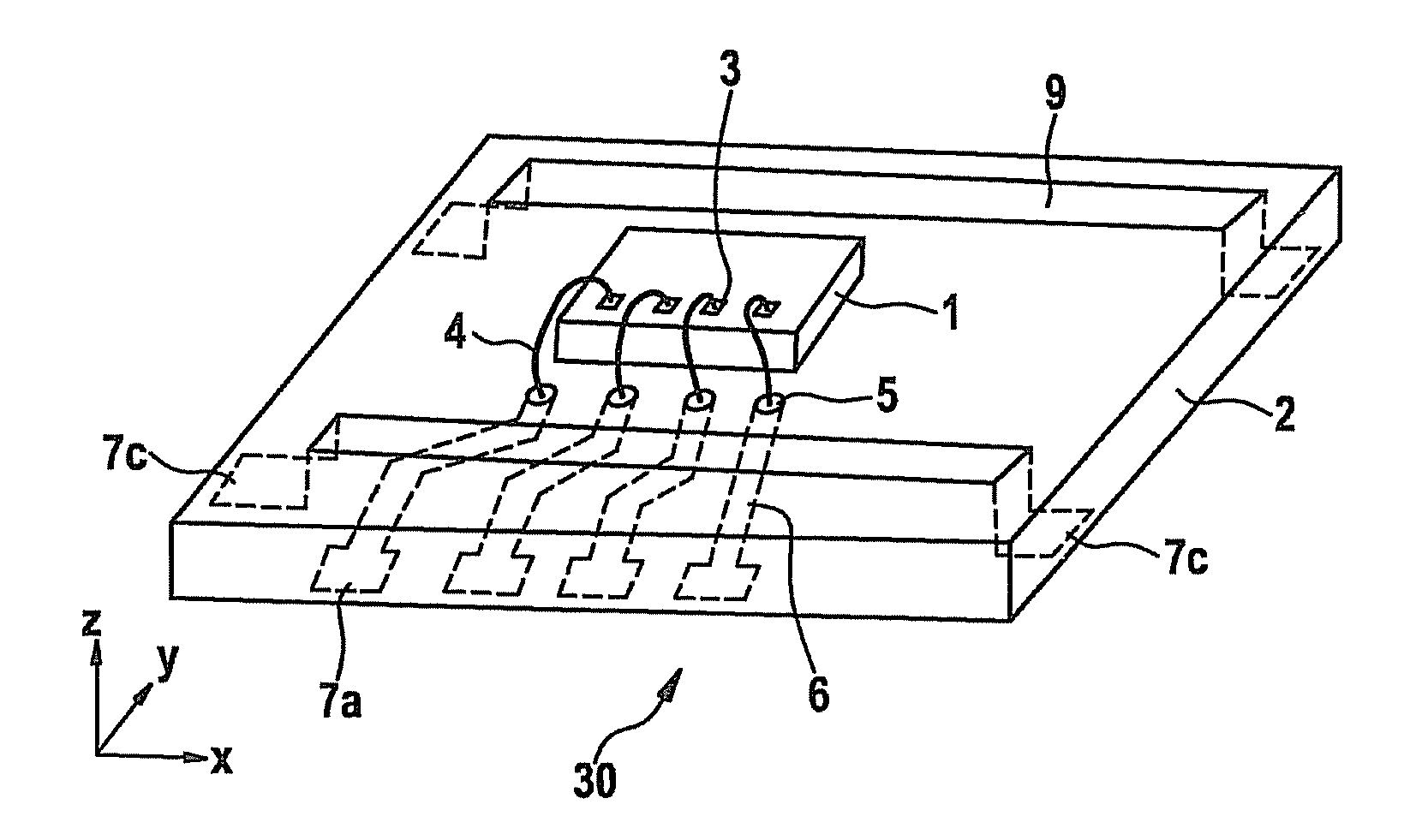
[0020]FIG. 1 shows a perspective view of a magnetic field sensor 10 according to a first exemplary embodiment of the present invention. Magnetic field sensor 10 includes a sensor element 1 mounted on, e.g., glued to, a printed circuit board 2.

[0021]Sensor element 1 is designed as a microsystem, i.e., the sensor structure for generating a sensor signal corresponding to the size of the magnetic field to be measured is provided monolithically on a semiconductor chip made of silicon, for example. Sensor element 1 in this exemplary embodiment is designed as a Hall sensor and generates an analog signal corresponding to the z component of the magnetic field at the sensor location. This analog signal is low-pass filtered and converted to a digital sensor signal by an analog-digital converter. In the present example, this further processing of the analog signal is implemented by a data processing unit integrated into sensor element 1. However, it is also possible to provide a separate module...


PUM


Abstract

A magnetic field sensor for measuring a magnetic field at a sensor location has a printed circuit board, including electrically insulating material; a magnetic field sensor element situated on the printed circuit board and connected via electrical contacts to first printed conductors provided on the printed circuit board; and at least one second printed conductor for generating a test magnetic field, the second printed conductor being provided on the printed circuit board and generating a predetermined test magnetic field when a calibration current is applied at the sensor location.

Description

FIELD OF THE INVENTION[0001]The present invention relates to a magnetic field sensor and in particular the calibration of such a sensor.BACKGROUND INFORMATION[0002]Various micromechanical magnetic field sensors which convert an interaction between an electrical current and the magnetic field into a force are available. German Patent No. DE 198 27 056, for example, describes a micromagnetic field sensor, in which a movement of a sensor structure induced by the Lorentz force is detected capacitively via comb-type electrodes. The Lorentz force is utilized in that a lateral movement of the free-floating structure is induced by a current, which is impressed upon an electrical conductor (free-floating) and an externally applied magnetic field.[0003]Furthermore, there are conventional micromagnetic field sensors, which utilize the Hall effect occurring in conductors through which a current flows in the presence of an external magnetic field. Electrons in the conductors are deflected by the...

Claims


Application Information

Patent Timeline
Patent Type & Authority Patents(United States)
IPC IPC(8): G01R33/02G01R33/00
CPCG01R33/0035H01L2224/48091H01L2224/48227H01L2924/00014G01R33/0017G01R33/0286
Inventor LAMMEL, GERHARDWEISS, STEFAN
Owner ROBERT BOSCH GMBH
Why Eureka
Try Eureka