Contact lens and method of manufacture to improve sensor sensitivity
a technology which is applied in the field of contact lens and sensor sensitivity improvement, can solve the problems of excessive clf polymer over the sensor, and achieve the effects of reducing the relative cost of chips, and reducing the cost of chips
- Summary
- Abstract
- Description
- Claims
- Application Information
AI Technical Summary
Benefits of technology
Problems solved by technology
Method used
Image
Examples
Embodiment Construction
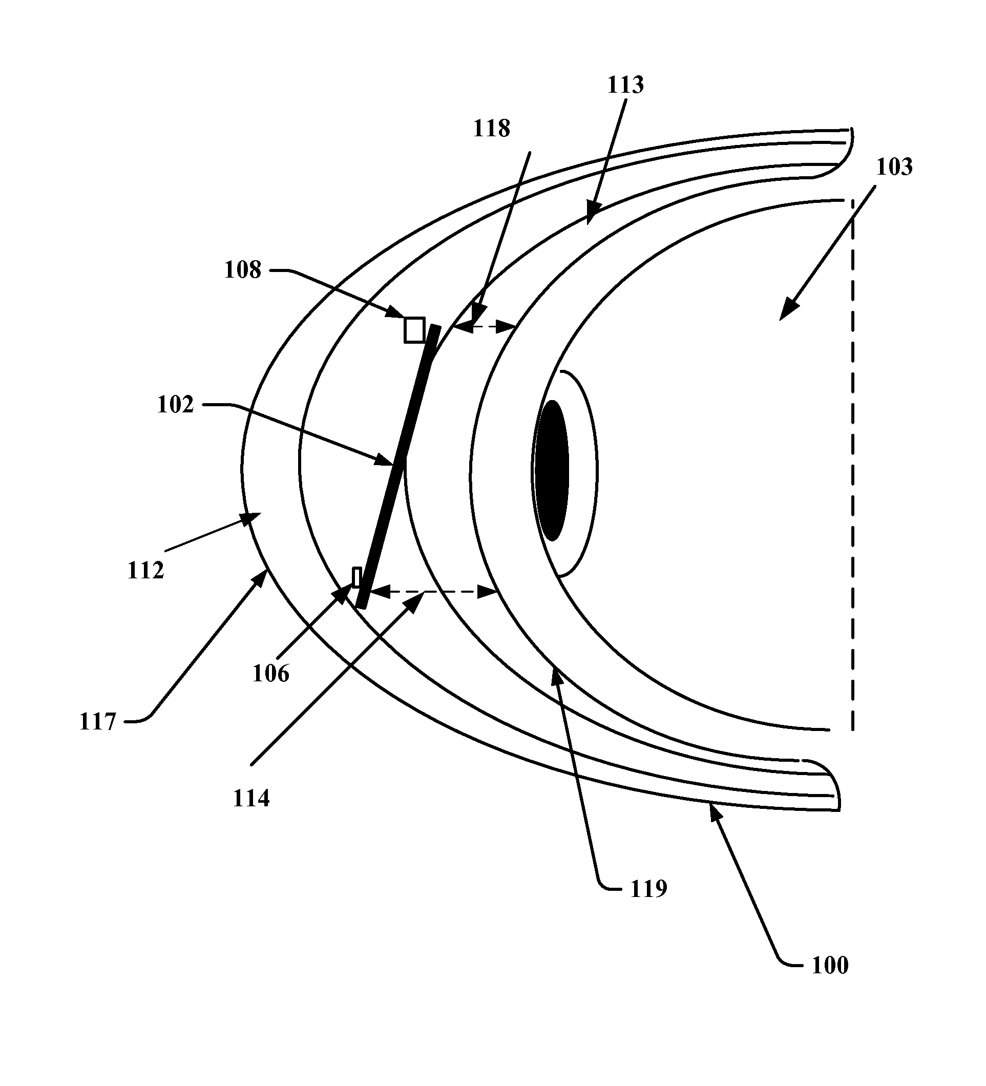
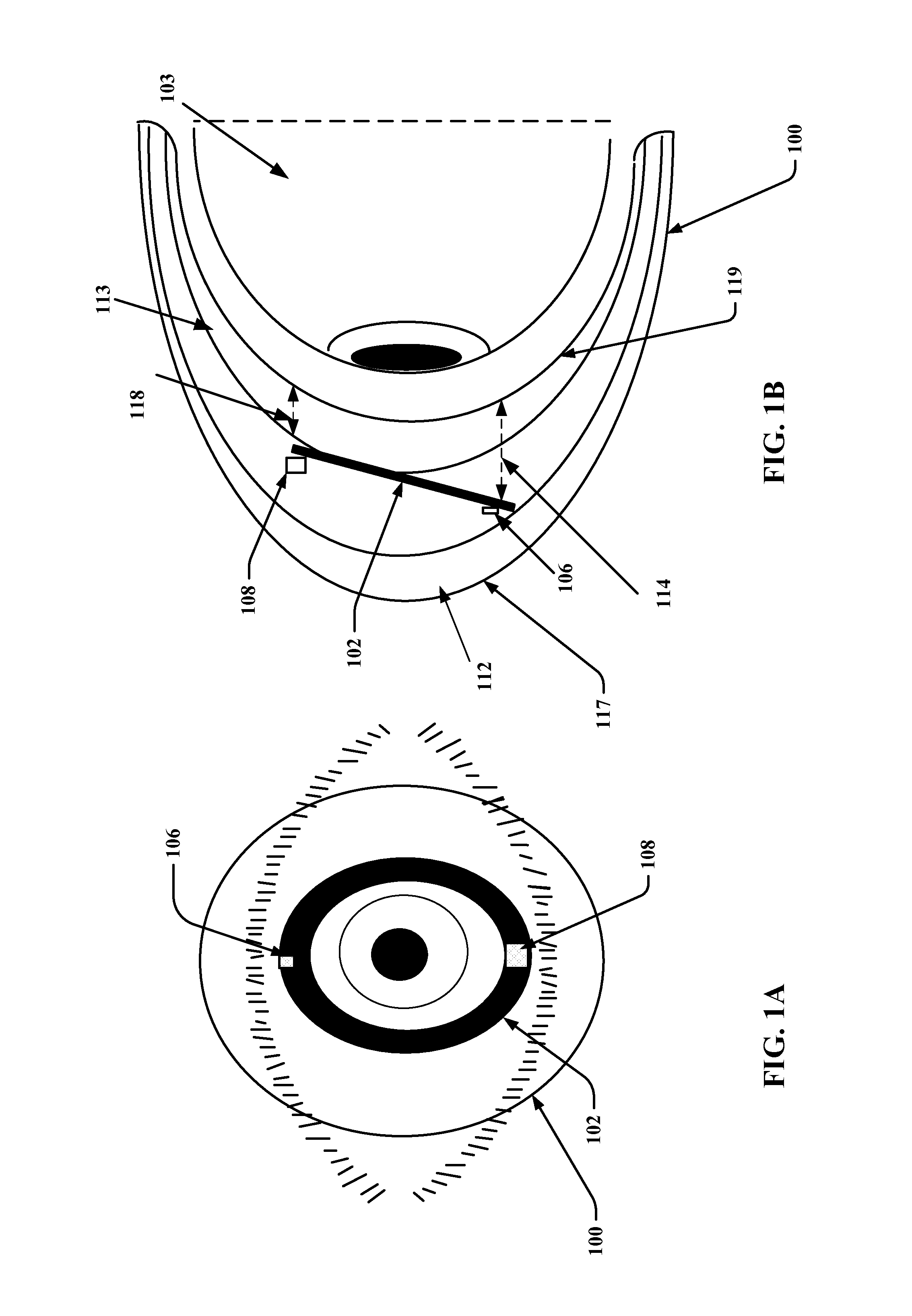
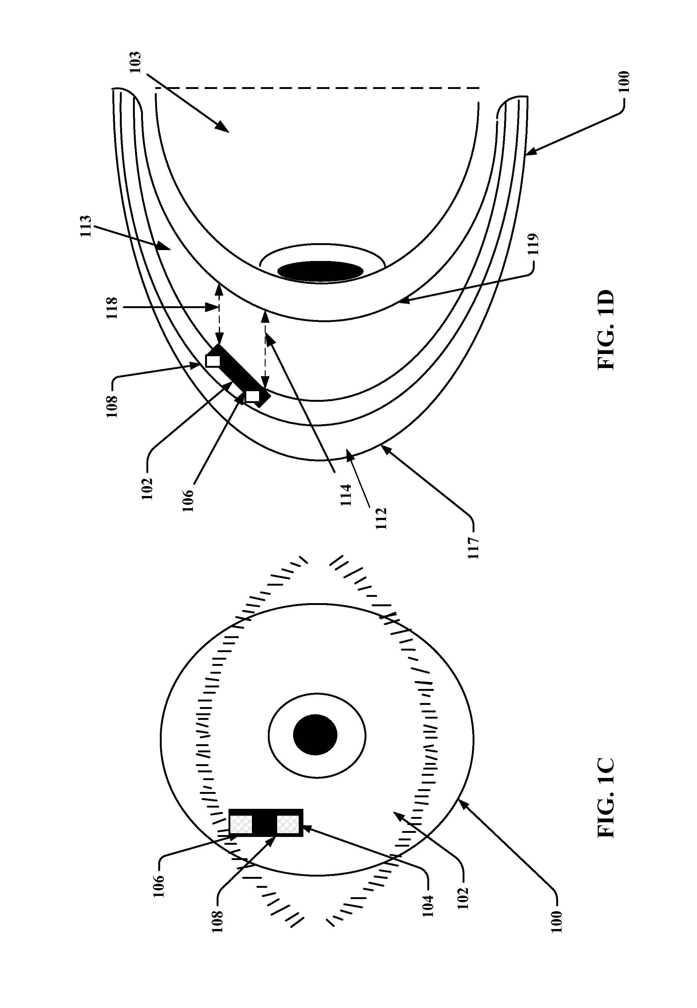
[0029]Turning first to FIGS. 1A, 1B, 1C, 1D and 1E, contact lens 100 can include an electronics substrate 102. In various aspects, as shown in FIG. 1E, the electronics substrate 102 can be angled relative to a base of the contact lens such that a first region of the electronics substrate 102 near position 116 is closer to a top surface 117 of the contact lens 100 and the second region of the electronics substrate 102 near position 120 is closer to the base 119 of the contact lens. In various aspects, with reference to FIGS. 1A, 1B, 1C, 1D, 1E, 1F, 1G, 1H, 1I and / or 1J, the electronics substrate 102 can be referred to interchangeably as slanted, angled or positioned at an incline.
[0030]As shown in FIGS. 1A and 1B, the electronics substrate 102 can be substantially ring-shaped. For example, the electronics substrate 102 can have an inner diameter that is approximately 8 millimeters and / or an outer diameter that is within the range of about 10-14 millimeters. It is to be appreciated th...
PUM
 Abstract
Description
Claims
Application Information
 - R&D
- Intellectual Property
- Life Sciences
- Materials
- Tech Scout
- Unparalleled Data Quality
- Higher Quality Content
- 60% Fewer Hallucinations
Browse by: Latest US Patents, China's latest patents, Technical Efficacy Thesaurus, Application Domain, Technology Topic, Popular Technical Reports.
© 2025 PatSnap. All rights reserved.Legal|Privacy policy|Modern Slavery Act Transparency Statement|Sitemap|About US| Contact US: help@patsnap.com


