
Semiconductor photo-detecting device

a technology of semiconductors and photo-detecting devices, which is applied in the direction of semiconductor devices, sustainable manufacturing/processing, climate sustainability, etc., can solve the problems of low detection efficiency, low detection efficiency, and low photo-detection efficiency, and achieve high photo-detection efficiency

Active Publication Date: 2015-10-27
SEOUL VIOSYS CO LTD
View PDF1 Cites 2 Cited by
  • Summary
  • Abstract
  • Description
  • Claims
  • Application Information

AI Technical Summary

Benefits of technology

This patent describes a photo-detecting device that can efficiently detect light in a specific wavelength range, such as UV light. The device has a light absorption layer with improved crystallinity that reduces the effect of visible light and increases the ratio of UV light to visible light detection. The device also includes a low-current blocking layer to improve its responsivity to visible light and achieve better photo-detection efficiency and reliability. Additionally, the device reduces the adverse effect of micro-currents induced by reaction to visible light.

Problems solved by technology

However, the semiconductor photo-detecting devices may require high voltage for operation and have low detection efficiency.
Particularly, when the semiconductor photo-detecting devices for detecting UV light are manufactured using silicon, photo-detection efficiency may decrease due to the silicon being sensitive not only to UV light but also to visible and infrared light.
In addition, UV light detecting devices using silicon may be thermally and chemically unstable.
In a structure including an AlGaN light absorption layer and a GaN buffer layer, when the AlGaN light absorption layer has an Al composition of 25% or more, or a thickness of 0.1 μm or more, cracks may be generated in the light absorption layer, thereby causing a yield decrease.
Specifically, when the thickness of the AlN layer is less than about 100 Å, photo-detection characteristics may be improved but it may be difficult to completely prevent cracks, and when the thickness of the AlN layer exceeds about 100 Å, cracks may be prevented, but photo-detection characteristics may be deteriorated.
In addition, GaN, InGaN, and AlGaN layers used as a light absorption layer in typical nitride-based semiconductor photo-detecting devices may have intrinsic defects and allow current flow in the devices in response to visible light, but not UV light due to such defects.
That is, the typical semiconductor photo-detecting devices may allow low current flow in response to visible light but not UV light, thereby, deteriorating detection accuracy.

Method used


Image

  • Semiconductor photo-detecting device
  • Semiconductor photo-detecting device
  • Semiconductor photo-detecting device

Examples


Embodiment Construction

[0024]In the following description, for the purposes of explanation, numerous specific details are set forth in order to provide a thorough understanding of various exemplary embodiments. It is apparent, however, that various exemplary embodiments may be practiced without these specific details or with one or more equivalent arrangements. In other instances, well-known structures and devices are shown in block diagram form in order to avoid unnecessarily obscuring various exemplary embodiments.

[0025]In the accompanying figures, the size and relative sizes of layers, films, panels, regions, etc., may be exaggerated for clarity and descriptive purposes. Also, like reference numerals denote like elements.

[0026]When an element or layer is referred to as being “on,”“connected to,” or “coupled to” another element or layer, it may be directly on, connected to, or coupled to the other element or layer or intervening elements or layers may be present. When, however, an element or layer is re...


PUM


Abstract

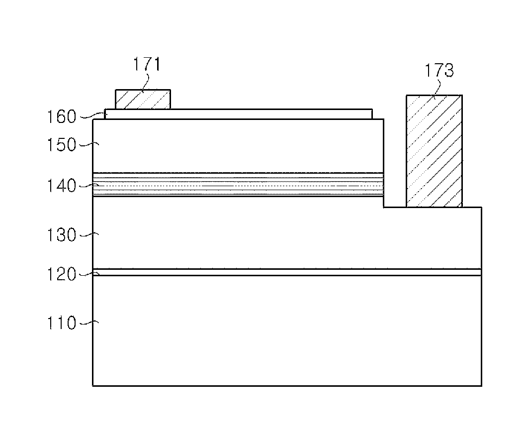
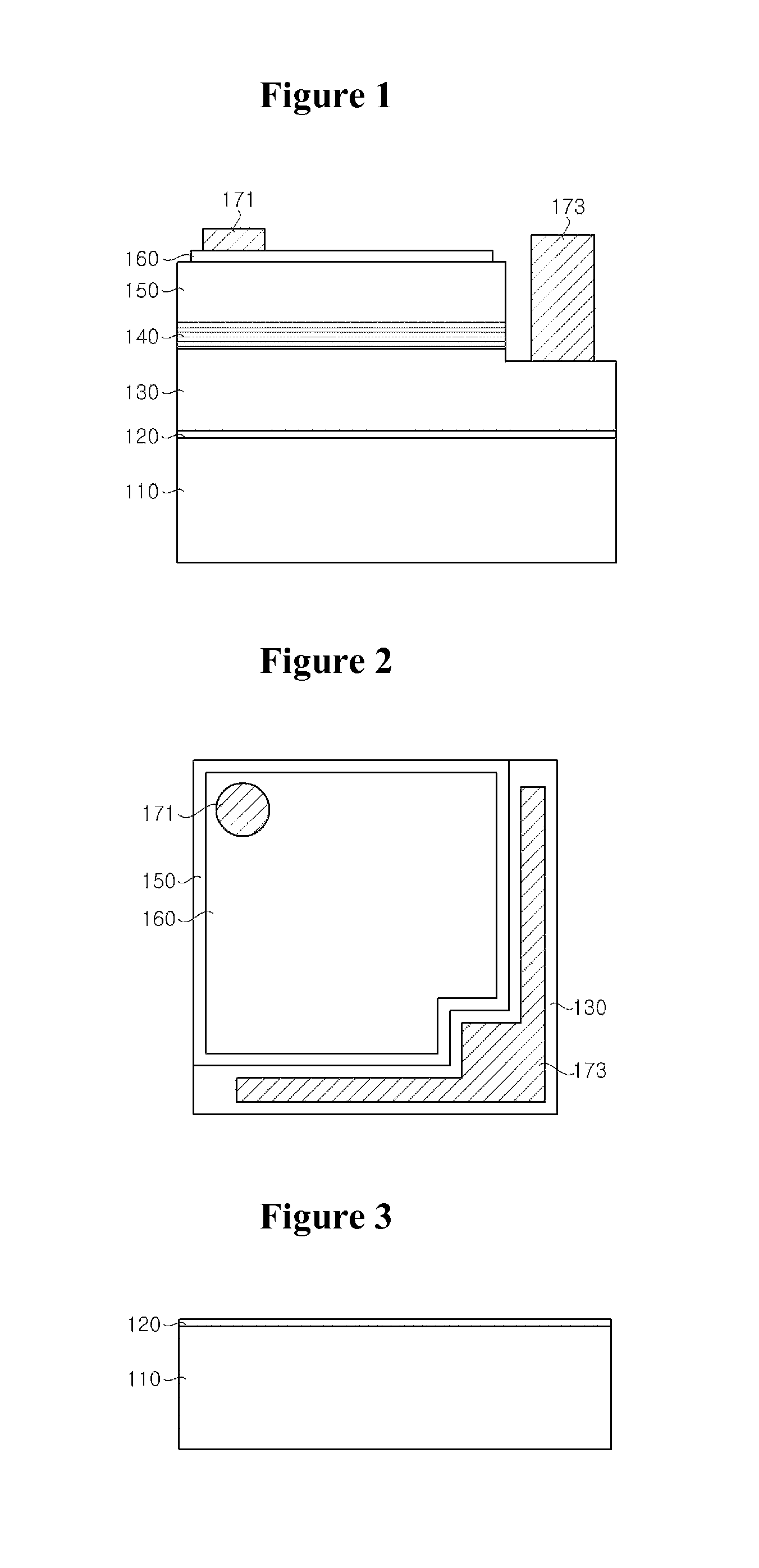
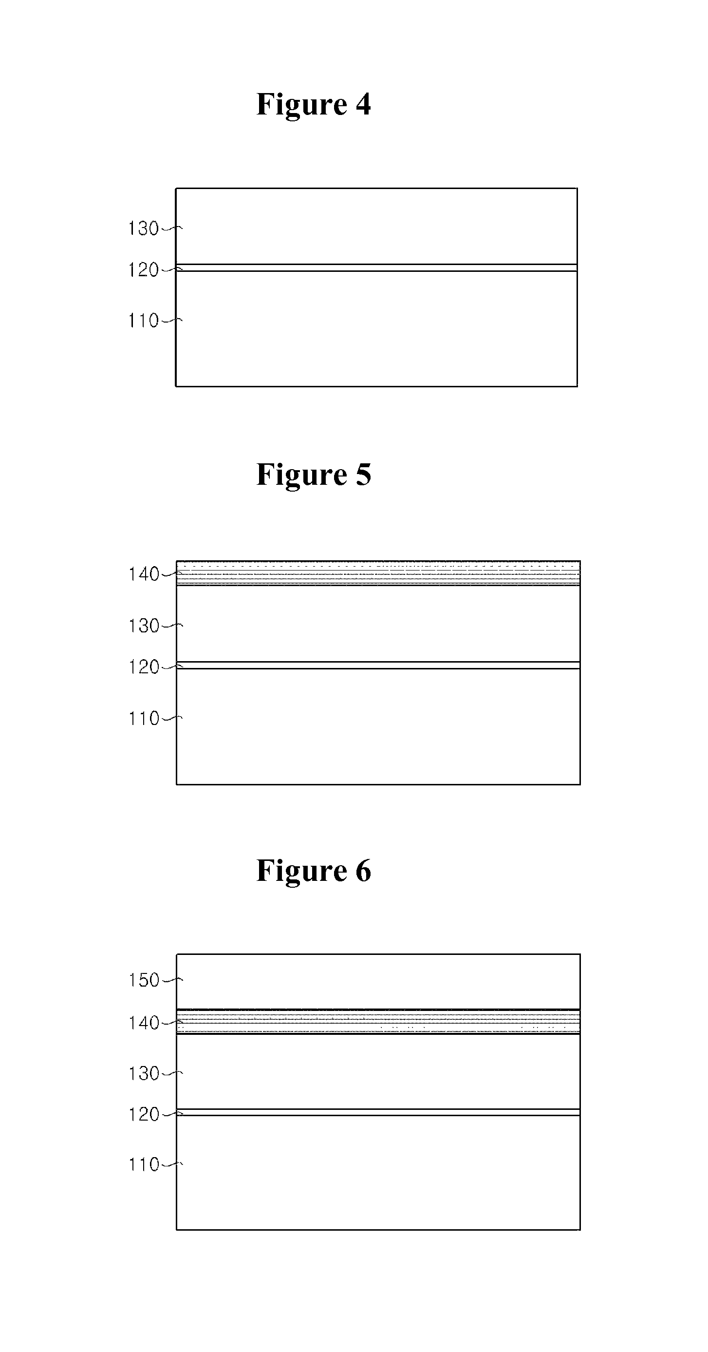
A photo-detecting device includes a first nitride layer, a low-current blocking layer disposed on the first nitride layer, a light absorption layer disposed on the low-current blocking layer, and a Schottky junction layer disposed on the light-absorption layer. The low-current blocking layer includes a multilayer structure.

Description

CROSS-REFERENCE TO RELATED APPLICATION[0001]This application claims priority from and the benefit of Korean Patent Application No. 10-2013-0113854, filed on Sep. 25, 2013, which is incorporated by reference for all purposes as if fully set forth herein.BACKGROUND[0002]1. Field[0003]Exemplary embodiments relate to a semiconductor photo-detecting device. More particularly, exemplary embodiments relate to a semiconductor photo-detecting device with excellent detection efficiency for a specific wavelength of light.[0004]2. Discussion of the Background[0005]Semiconductor photo-detecting devices operate on the principle that current is induced by illuminated light. In particular, semiconductor photo-detecting devices for detecting ultraviolet (UV) light may be used in a variety of fields, such as business, medical science, defense industry, communications, etc. The semiconductor photo-detecting devices are based on the principle that a depletion region is formed by the separation of elect...

Claims


Application Information

Patent Timeline
Patent Type & Authority Patents(United States)
IPC IPC(8): H01L31/0328H01L31/0336H01L31/072H01L31/0304H01L31/108H01L31/109H01L31/18
CPCH01L31/108H01L31/03044H01L31/03048H01L31/1848H01L31/1856H01L31/101H01L31/18Y02P70/50H01L31/09Y02E10/544
Inventor PARK, KI YONKIM, HWA MOKLEE, KYU HOLEE, SUNG HYUNKIM, HYUNG KYU
Owner SEOUL VIOSYS CO LTD
Learn More