Crystallinity evaluation method, crystallinity evaluation device, and computer software thereof

a crystallinity evaluation and crystallinity technology, applied in the direction of fluid pressure measurement by mechanical elements, vibration measurement in solids, blast furnaces, etc., can solve the problem of poor physical grounds, inability to accurately evaluate/analyze crystallinity by using there parameters, and inability to accurately evaluate/analyze crystallinity

Inactive Publication Date: 2015-09-01
JOLED INC +1
View PDF30 Cites 4 Cited by
  • Summary
  • Abstract
  • Description
  • Claims
  • Application Information

AI Technical Summary

Benefits of technology

[0036]The present disclosure according to one or more exemplary embodiments or features disclosed herein provide a crystallinity evaluation method and a crystallinity evaluation device each capable of correctly evaluating crystallinity of a crystalline semiconductor film having high-mobility properties without mobility variation, and a computer software for them.

Problems solved by technology

However, the methods disclosed in the above-described Patent Literatures 4 and 5 fail to correctly evaluate (analyze) crystallinity of crystalline silicon films.
However, these parameters are affected by measurement conditions, a sample state, and the like, and therefore do not always reflect only crystallinity.
It is therefore impossible to correctly evaluate / analyze crystallinity by using there parameters.
However, this analysis method has poor physical grounds and therefore has a difficulty in correctly analyzing a Raman spectrum.
In other words, it is impossible to correctly evaluate (analyze) crystallinity by using this analysis method.
However, this analysis method also has a problem of poor reproducibility of experimental results.
In other words, it is impossible to correctly evaluate (analyze) crystallinity by using this analysis method.

Method used


Image

  • Crystallinity evaluation method, crystallinity evaluation device, and computer software thereof
  • Crystallinity evaluation method, crystallinity evaluation device, and computer software thereof
  • Crystallinity evaluation method, crystallinity evaluation device, and computer software thereof

Examples


embodiment 1

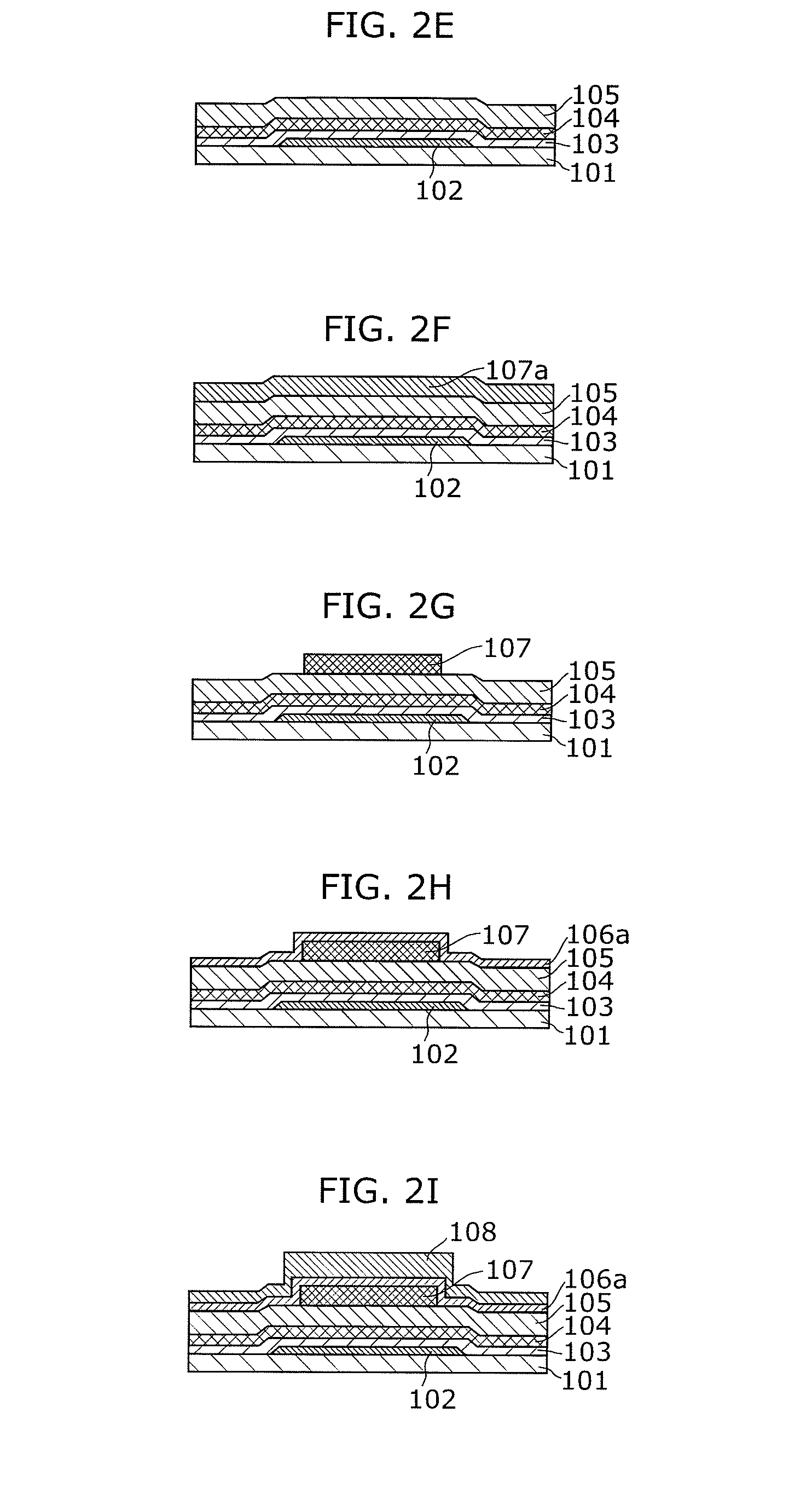
[0106]The following describes a TFT and a manufacturing method thereof according to the present disclosure based on embodiments, but the present disclosure is based on the claims. Therefore, although structural elements not described in the claims among the structural elements in the following embodiments are not always necessary to solve the problems, such structural elements are also described as being included in more desirable embodiments. It should also be noted that each of the figures is a schematic diagram and is not always depicted exactly.

[0107]First, the description is given for a structure of the TFT 100 according to the present embodiment. FIG. 1 is a cross-sectional view schematically showing a structure of a TFT according to Embodiment 1.

[0108]The TFT 100 shown in FIG. 1 is a channel-protection bottom-gate TFT. The TFT 100 includes: a substrate 101; a gate electrode 102 formed on the substrate 101; a gate insulating film 103 formed on the gate electrode 102; a crystal...

embodiment 2

[0240]The following describes a crystallinity evaluation method of evaluating crystallinity of a semiconductor film (hereinafter, referred to as a “film quality analysis method”) according to Embodiment 2 in detail with reference to the drawings.

[0241]According to the present embodiment, Raman spectrometry for a crystalline silicon film is performed on a specimen 307 (not shown) by using the Raman spectrometer shown in FIG. 3.

[0242]Here, the specimen 307 is a crystalline silicon film formed by forming a base coat layer and amorphous silicon film (a-Si film) on a glass substrate and then crystallizing the amorphous silicon film to form the crystalline silicon film. The base coat film is, for example, a film having a low thermal conductivity, such as a silicon oxide film or a silicon nitride film having a thickness ranging approximately from 100 nm to 1 μm. The amorphous silicon film (a-Si film) is formed, for example, by depositing a film having a thickness ranging approximately from...

example 1

[0264]According to the present example, a result of analyzing a Raman spectrum of a crystalline silicon film manufactured by crystallizing an a-Si film by using continuous wave (CW) laser is described.

[0265]A specimen (specimen 307) is generated by forming a silicon nitride film (base coat layer) of approximately 200 nm and an a-Si film of approximately 50 nm on a glass substrate, and then crystallizing them by CW laser. The a-Si crystallization is performed by using CW laser with a wavelength of 532 nm and a power density of 70 Kw / cm2.

[0266]Here, as a plurality of such specimens 307, samples for which a scan speed of the laser is varied to vary the crystalline structure are manufactured. In more detail, samples having respective crystalline silicon films for which solid-phase growth, partial-melt growth, and melt growth are performed, respectively. Here, in order to form crystalline silicon films for which solid-phase growth, partial partial-melt growth, and melt growth are perform...


PUM

PropertyMeasurementUnit
full-width at half maximumaaaaaaaaaa
thicknessaaaaaaaaaa
thicknessaaaaaaaaaa

Abstract

A crystallinity evaluation method of evaluating crystallinity of a semiconductor film formed above a substrate includes following steps. First, a peak waveform of a Raman band in a Raman spectrum of the semiconductor film is obtained using Raman spectrometry. The Raman band corresponds to a phonon mode unique to the semiconductor film. The peak waveform is a wavelength range having a peak of the Raman band. Next, a first waveform is generated by fitting the obtained peak waveform by Gauss function. Then, a peak value of the first waveform is extracted. Then, a second waveform is generated by fitting the obtained peak waveform by Lorenz function based on the extracted peak value. Then, a peak value, a FWHM, and / or a wavelength indicating the peak value regarding the generated second waveform are obtained. Then, crystallinity of the semiconductor film is evaluated based on the obtained information.

Description

CROSS REFERENCE TO RELATED APPLICATIONS[0001]This is a continuation application of International Application No. PCT / JP2012 / 00752 filed on Feb. 3, 2012, designating the United States of America, which is based on and claims priority of Japanese Patent Applications Nos. 2011-048369 filed on Mar. 4, 2011 and 2011-225375 filed on Oct. 12, 2011. The entire disclosures of the above-identified applications, including the specifications, drawings and claims are incorporated herein by reference in their entirety.TECHNICAL FIELD[0002]One or more exemplary embodiments disclosed herein relate generally to crystallinity evaluation methods, crystallinity evaluation devices, and their computer software, regarding crystalline semiconductor films.BACKGROUND ART[0003]For example, there are electronic devices such as a television receiver using an organic electro-luminescence (EL) display or a liquid crystal display. In such an electronic device, luminescence elements arranged in a matrix to form an ...

Claims


Application Information

Patent Timeline
Patent Type & Authority Patents(United States)
IPC IPC(8): G01N21/65H01L21/66H01L29/66C30B33/00
CPCG01N21/65H01L22/12H01L29/66765C30B33/00H01L2924/0002H01L2924/00
Inventor KAWASHIMA, TAKAHIROKAWACHI, GENSHIROODA, TOMOHIKONISHITANI, HIKARU
Owner JOLED INC
Why Eureka
Try Eureka