Signal transfer device
a technology of signal transfer and input/output logic, applied in the direction of logic circuit coupling/interface arrangement, digital transmission, baseband system details, etc., can solve the problem of inability to provide a solution, etc., and achieve the effect of quick solving the input/output logic mismatch
- Summary
- Abstract
- Description
- Claims
- Application Information
AI Technical Summary
Benefits of technology
Problems solved by technology
Method used
Image

Examples
first embodiment
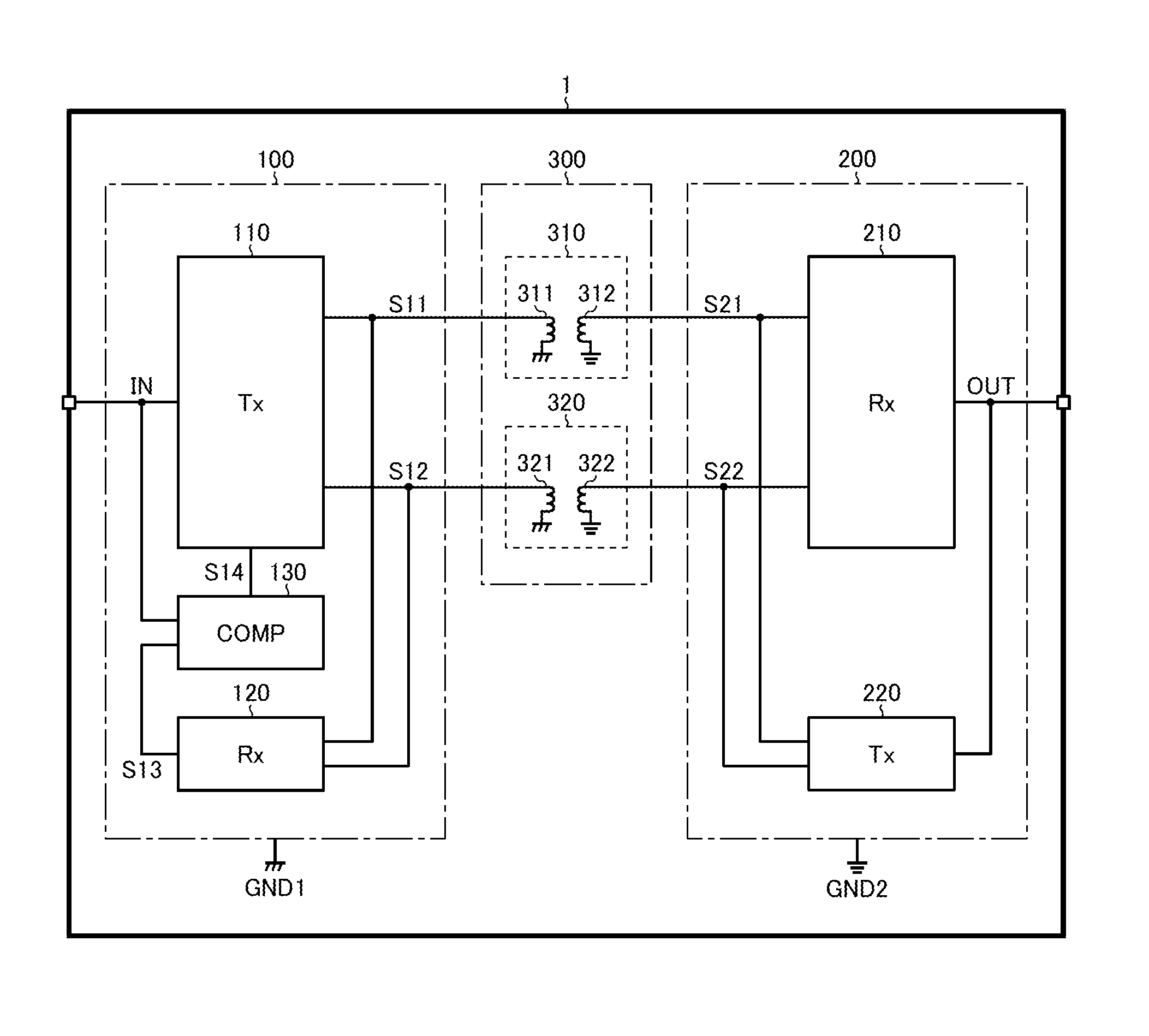
[0047]FIG. 1 is a block view showing a first embodiment of a signal-transferring device. The signal-transferring device 1 of the present embodiment is a semiconductor integrated circuit device for generating an output signal OUT to a secondary-side circuit (not shown) that operates on a GND2 basis in accordance with an input signal IN from a primary-side circuit (not shown) that operates on a GND1 basis, and has a first circuit 100, a second circuit 200, and a third circuit 300. The signal-transferring device 1 can be widely applied to applications in general (motor drivers that handle high voltage, DC / DC converters, and the like) that require signals to be transferred between a primary-side circuit and a secondary-side circuit while providing electrical insulation therebetween.
[0048]The first circuit 100 is a circuit block that operates on a GND1 basis, and includes a primary-side transmission unit 110, a primary-side receiving unit 120, and an input / output comparison unit 130. The...
first configuration example
[0114]FIG. 15 is a block view showing a first configuration example of the secondary-side receiving unit 210. The secondary-side receiving unit 210 of the present configuration example includes a comparison processing unit 211, mask processing units 212 and 213, a RS flip-flop 214, and an operational state assessment unit 215.
[0115]The comparison processing unit 211 is a circuit unit comparing a predetermined threshold voltage th of the third signal S21 and the fourth signal S22 to generate receiving signals S81a and S81b, and includes comparators 211a and 211b. The comparator 211a compares the third signal S21 applied to the non-inverted input terminal (+) and the threshold voltage Vth applied to the inverted input terminal (−), and generates a receiving signal SSla. The receiving signal S81a is at a high level when the third signal S21 is higher than the threshold voltage Vth, and is at a low level when the third signal S21 is lower than the threshold voltage Vth. The comparator 2...
second embodiment
[0132]FIG. 17 is a block view showing a second embodiment of the signal-transferring device. The signal-transferring device 1 of the second embodiment is essentially the same as the first embodiment above, and has a feature in which a transformer 330 has been added to the third circuit 300. In view of this addition, the same reference numerals as in FIG. 1 will be used for the same constituent elements as in the first embodiment, and a duplicative description will be omitted, and the second embodiment will be described below with emphasis on the characteristic portions.
[0133]The primary-side receiving unit 120 and the secondary-side transmission unit 220 above are changed to the primary-side transceiving unit 140 and the secondary-side transceiving unit 230, respectively, in accompaniment with the addition of the transformer 330 to the third circuit 300.
[0134]The primary-side transceiving unit 140 transmits a clock signal CLK to the secondary-side transceiving unit 230 by way of the...
PUM
 Abstract
Description
Claims
Application Information
 - R&D
- Intellectual Property
- Life Sciences
- Materials
- Tech Scout
- Unparalleled Data Quality
- Higher Quality Content
- 60% Fewer Hallucinations
Browse by: Latest US Patents, China's latest patents, Technical Efficacy Thesaurus, Application Domain, Technology Topic, Popular Technical Reports.
© 2025 PatSnap. All rights reserved.Legal|Privacy policy|Modern Slavery Act Transparency Statement|Sitemap|About US| Contact US: help@patsnap.com