Organic light emitting diode display and method of manufacturing the same

a light-emitting diode and organic technology, applied in the direction of thermoelectric device junction materials, electrical apparatus, semiconductor devices, etc., can solve the problems of significantly reducing the life reducing the performance of the display device, etc., to improve imaging quality, prevent the formation of pores, and dispose of donor films stably

Active Publication Date: 2015-04-14
SAMSUNG DISPLAY CO LTD
View PDF16 Cites 0 Cited by
  • Summary
  • Abstract
  • Description
  • Claims
  • Application Information

AI Technical Summary

Benefits of technology

[0012]The present invention has been developed in an effort to provide an organic light emitting diode display structure and a method of manufacturing the same, in which gas generated during an organic layer imaging process by a laser-induced thermal imaging (LITI) method can be exhausted, and thus pores can be prevented from being generated in a pixel region on which an organic layer is imaged and an imaging film can be stably disposed.
[0018]The pixel defining layer may have the same height as the first electrode in a region around the first electrode and may have a plurality of grooves having the same height as the first electrode for preventing attachment of an imaging layer in a region between the sub-pixel regions.
[0019]The pixel defining layer may have the same height as the first electrode and may have a plurality of grooves havingae height that is smaller than the height of the first electrode for preventing attachment of an imaging layer in a region between the sub-pixel regions.
[0023]According to the exemplary embodiments of the present invention, it is possible to exhaust gas generated in a pixel region during an imaging process by laser-induced thermal imaging during a process of manufacturing an organic light emitting diode display, to prevent pores from being generated, and to stably dispose a donor film on a substrate to improve imaging quality.

Problems solved by technology

However, in the laser-induced thermal imaging process, when the donor film is laminated on the organic light emitting diode display, there is concern that micropores may be formed in an imaging material of the pixel region which reduces performance of a display device and significantly reduces a life-span.

Method used


Image

  • Organic light emitting diode display and method of manufacturing the same
  • Organic light emitting diode display and method of manufacturing the same
  • Organic light emitting diode display and method of manufacturing the same

Examples


Embodiment Construction

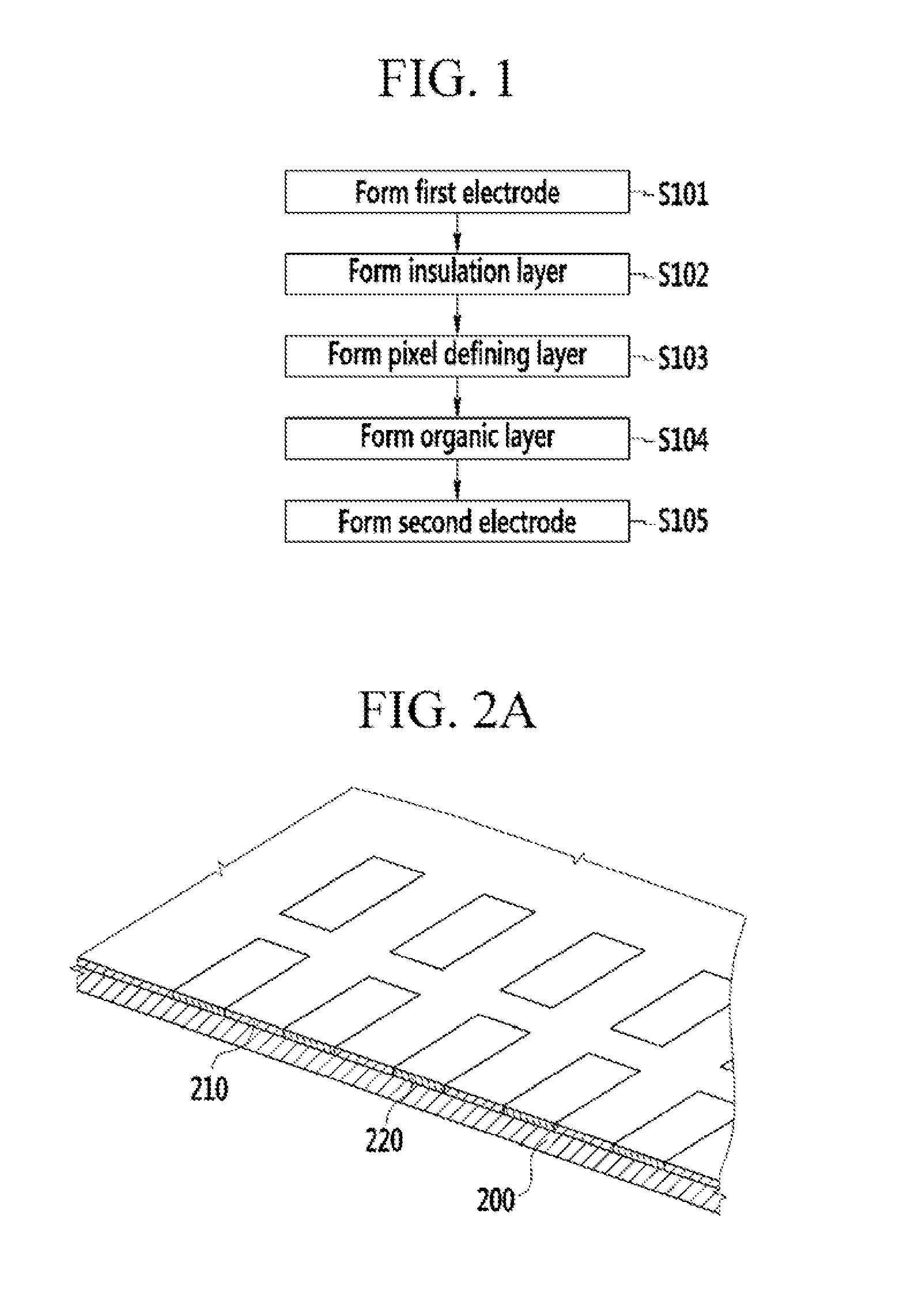
[0049]Hereinafter, exemplary embodiments of the present invention will be described more fully with reference to the accompanying drawings, in which exemplary embodiments of the invention are shown. As those skilled in the art will realize, the described embodiments may be modified in various different ways, all without departing from the spirit or scope of the present invention.

[0050]In addition, in various exemplary embodiments, the same reference numerals are used with respect to the constituent elements having the same constitution, and the constituent elements are representatively described in the first exemplary embodiment, and in the other exemplary embodiments, only constitution that is different from the first exemplary embodiment is described.

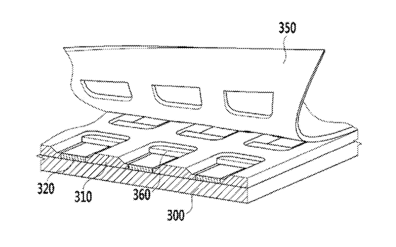
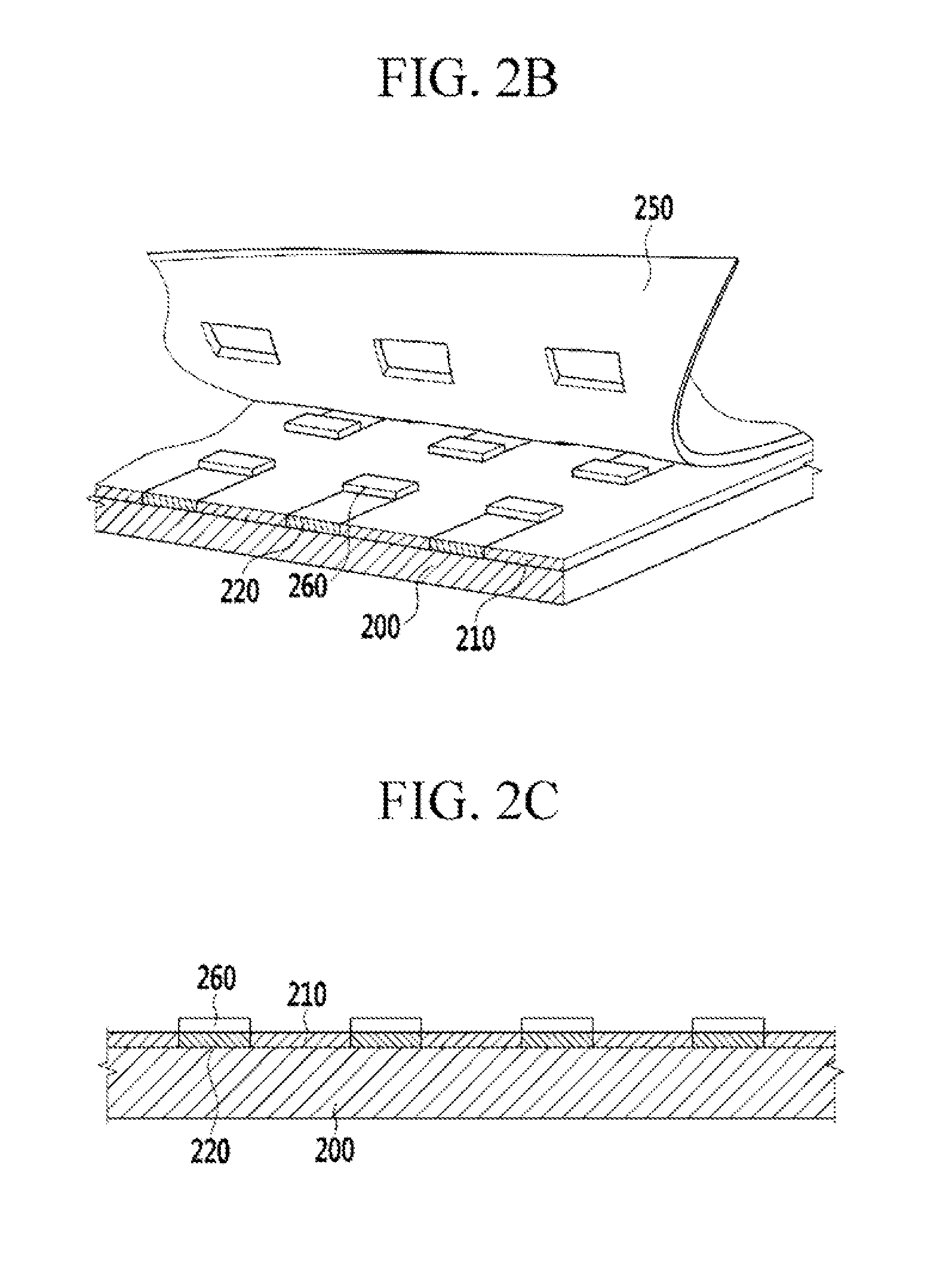
[0051]It is noted that the drawings are schematic and are not dimensionally illustrated. Relative dimensions and ratios of portions of the drawings are exaggerated or reduced in size for clarity and convenience in the drawings, and a ...


PUM


Abstract

A method of manufacturing an organic light emitting diode display according to an exemplary embodiment of the present invention includes: forming a first electrode on a substrate; forming an insulation layer on the first electrode; etching the insulation layer to expose the first electrode so as to form a pixel defining layer having the same height as the first electrode; forming an organic layer including one or more emission layers on the first electrode of a sub-pixel region defined by the pixel defining layer by applying a laser-induced thermal imaging (LITI) method; and forming a second electrode on the organic layer.

Description

CLAIM OF PRIORITY[0001]This application claims priority to and the benefit of Korean Patent Application No. 10-2013-0033064 filed in the Korean Intellectual Property Office on Mar. 27, 2013, the entire contents of which are incorporated herein by reference.BACKGROUND OF THE INVENTION[0002]1. Field of the Invention[0003]The present invention relates to an organic light emitting diode (OLED) display and a method of manufacturing the same, and more particularly, to an organic light emitting diode display and a method of manufacturing the same, which include an organic layer imaging process by a laser-induced thermal imaging (LITI) method.[0004]2. Description of the Related Art[0005]A full-color organic light emitting diode display includes a first electrode pattern formed on a substrate. In a lower light emitting type organic light emitting diode display, the first electrode is a transparent electrode. In an upper light emitting type organic light emitting diode display, the first elec...

Claims


Application Information

Patent Timeline
Patent Type & Authority Patents(United States)
IPC IPC(8): H01L29/08H01L51/52H01L51/56
CPCH01L51/5203H01L51/56H01L27/3246H01L51/0013H10K59/122H10K71/18H10K71/00H10K59/35H10K59/123H10K59/124H10K50/805
Inventor PRUSHINSKIY, VALERIYKIM, MIN-SOOHYUN, WON-SIKNA, HEUNG-YEOLSUN, JIN-WON
Owner SAMSUNG DISPLAY CO LTD
Why Eureka
Try Eureka