Lighting device
a technology of light source and light source, which is applied in the field of light source, can solve the problems of low durability of above-organic electroluminescence element and organic photoelectric conversion element, and achieve the effect of improving the durability of the entire lighting device and improving the durability
- Summary
- Abstract
- Description
- Claims
- Application Information
AI Technical Summary
Benefits of technology
Problems solved by technology
Method used
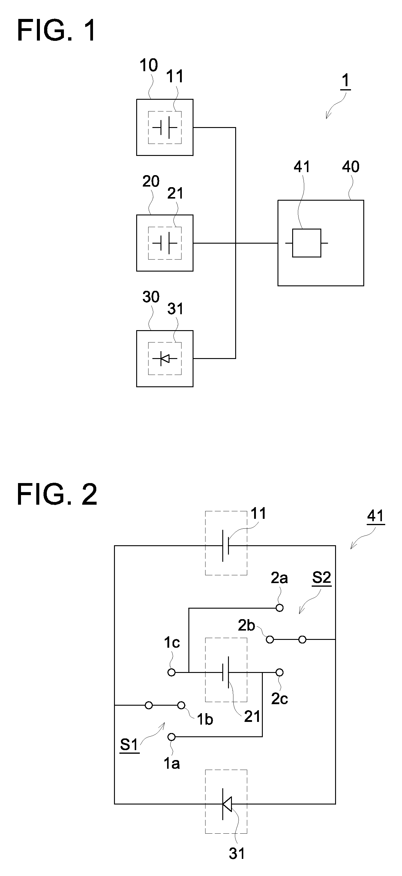
Image


Examples
examples
[0205]
[0206]A transparent conductive film composed of indium / tin oxide (ITO) was accumulated to a thickness of 110 nm on a PEN film substrate of a size of 10 cm×10 cm having a barrier layer (sheet resistance of 13Ω / □), which was then subjected to a patterning with 5 cm in width in the central part using a general photolithographic technique and hydrochloric etching, to form a flexible transparent substrate having a transparent electrode.
[0207]31>
[0208]The above flexible transparent substrate was attached to a commercially available spin coater, and then, the positive hole injection layer PEDOT (PEDOT: PEDOT / PSS, manufactured by Bayer Corp., BAYTRON P AI 4083) was spin-coated on the substrate (film thickness of about 40 nm), which was then heated by a hot plate at 200° C. for one hour, to prepare a positive hole injection layer. Further, the volume of the white light emitting composite having a composition below was adjusted to make 1 ml, which was then spin-coated on the above resul...
PUM
| Property | Measurement | Unit |
|---|---|---|
| reverse bias voltage | aaaaa | aaaaa |
| reverse bias voltage | aaaaa | aaaaa |
| voltage | aaaaa | aaaaa |
Abstract
Description
Claims
Application Information
 - R&D
- Intellectual Property
- Life Sciences
- Materials
- Tech Scout
- Unparalleled Data Quality
- Higher Quality Content
- 60% Fewer Hallucinations
Browse by: Latest US Patents, China's latest patents, Technical Efficacy Thesaurus, Application Domain, Technology Topic, Popular Technical Reports.
© 2025 PatSnap. All rights reserved.Legal|Privacy policy|Modern Slavery Act Transparency Statement|Sitemap|About US| Contact US: help@patsnap.com