
Drive circuit and display device

a drive circuit and display device technology, applied in the direction of pulse generators, pulse techniques, instruments, etc., can solve the problems of vsub>th /sub>, intensity variation, etc., and achieve the effect of improving uniformity of intensity, reducing intensity, and reducing the variation of a current flowing in an organic el element at the time of light emission

Inactive Publication Date: 2015-02-24
JOLED INC
View PDF30 Cites 0 Cited by
  • Summary
  • Abstract
  • Description
  • Claims
  • Application Information

AI Technical Summary

Benefits of technology

[0014]In view of the foregoing, it is desirable to provide a drive circuit capable of reducing a variation in the timing of a rise in an output voltage, and a display device including this drive circuit.
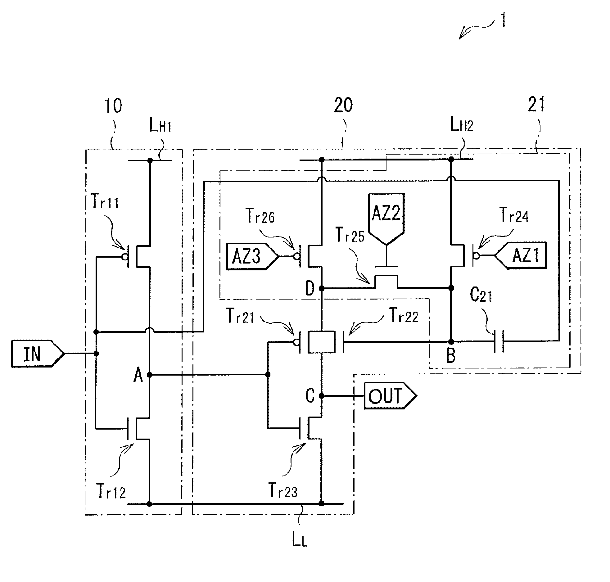
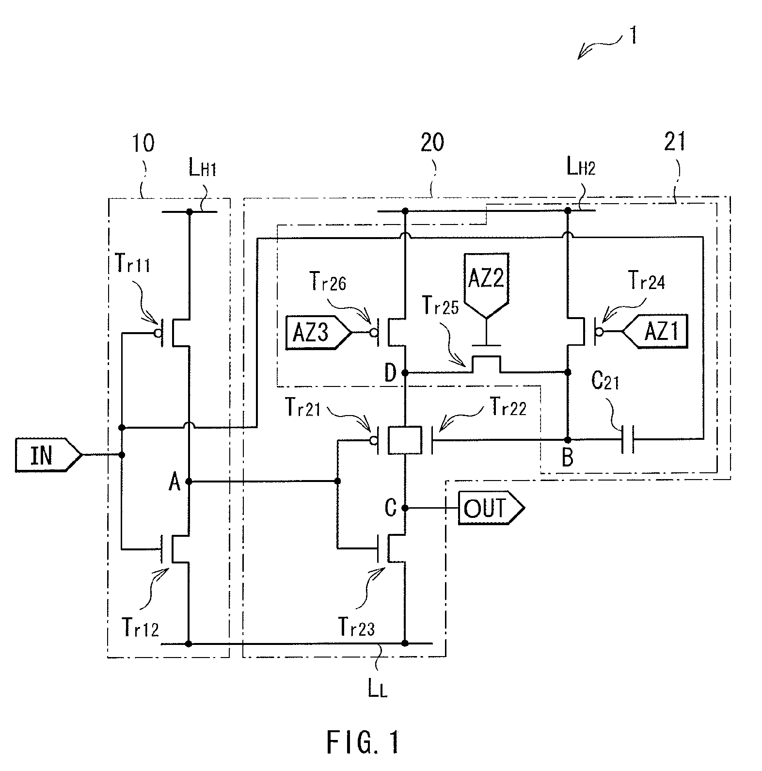
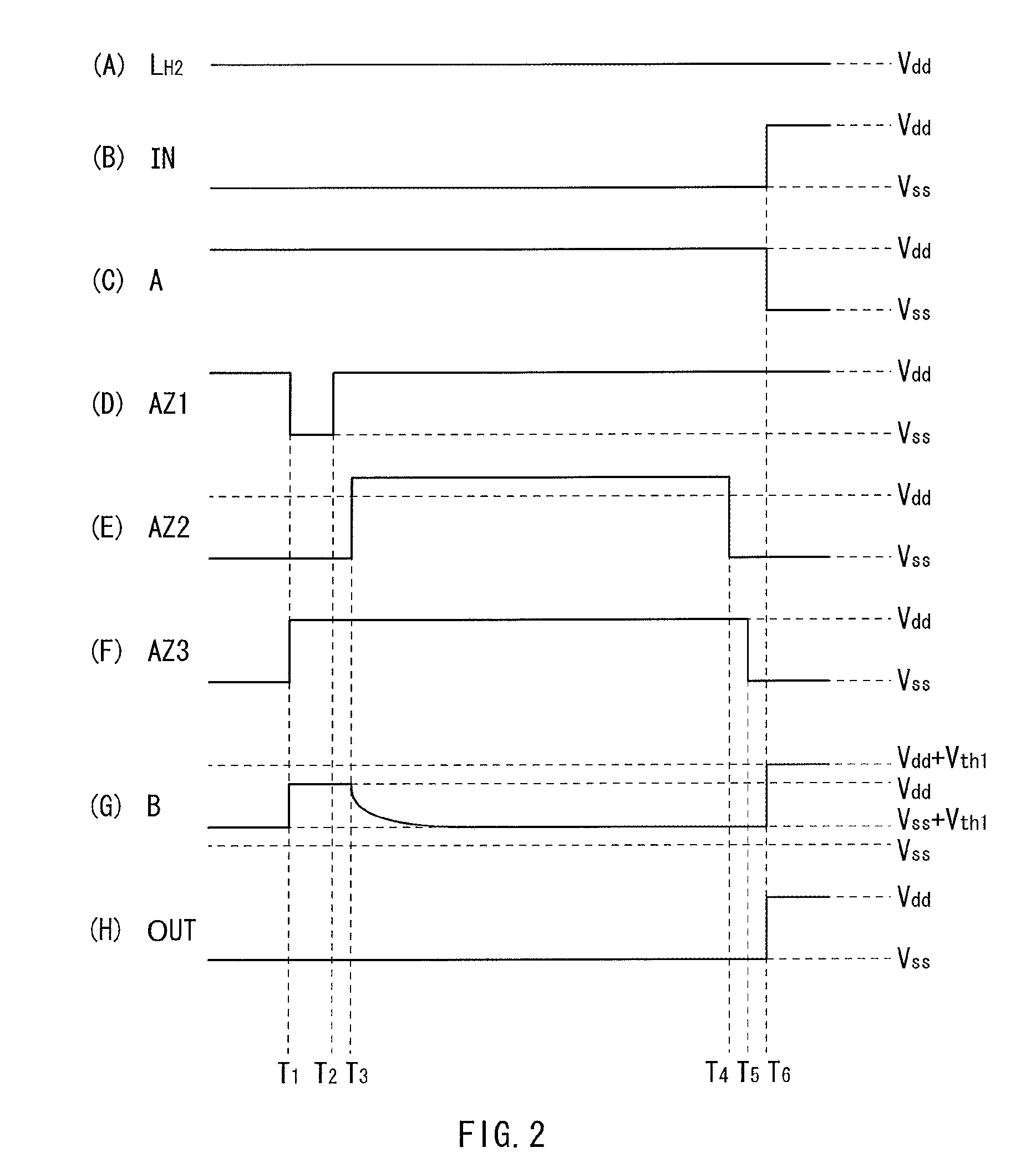
[0018]According to the above-described drive circuit and the display device of the embodiments, in one or both of the two gates of the CMOS transistor, the voltage corresponding to the threshold voltage of the CMOS transistor can be set as an offset. Thus, a variation can be reduced in timing of a rise in the output voltage of the drive circuit. Therefore, for example, in an organic EL display device, a variation in a current flowing in an organic EL element at the time of light emission can be reduced and thus, uniformity of intensity can be improved.

Problems solved by technology

Therefore, there is such a problem that when, for example, the timing of a rise in the voltage Vout of the output OUT varies and a mobility correction period ΔT varies by Δt1 or Δt2, a current Ids at the time of light emission varies by ΔIds as illustrated in, for example, FIG. 24, and this variation leads to a variation in intensity.
Incidentally, the problem of the variation in the threshold voltage Vth not only occurs in the scan circuit of the display device, but also similarly occurs in other device.

Method used


Image

  • Drive circuit and display device
  • Drive circuit and display device
  • Drive circuit and display device

Examples


application example

[0108]FIG. 17 illustrates an example of the entire structure of a display device 100 serving as an example of the application example of the buffer circuits 1 through 4 according to the above-described respective embodiments. This display device 100 includes, for example, a display panel 110 (display section) and a drive circuit 120 (drive section).

[0109](Display Panel 110)

[0110]The display panel 110 includes a display region 110A in which three kinds of organic EL elements 111R, 111G and 111B emitting mutually different colors are arranged two-dimensionally. The display region 110A is a region for displaying an image by using light emitted from the organic EL elements 111R, 111G and 111B. The organic EL element 111R is an organic EL element emitting red light, the organic EL element 111G is an organic EL element emitting green light, and the organic EL element 111B is an organic EL element emitting blue light. Incidentally, in the following, the organic EL elements 111R, 111G and 1...


PUM


Abstract

A drive circuit includes: an input-side inverter circuit and an output-side inverter circuit connected to each other in series and inserted between a high voltage line and a low voltage line. The output-side inverter circuit includes a CMOS transistor having a first gate and a second gate, in which a drain is connected to the high voltage line side and a source is connected to an output side of the output-side inverter circuit. The output-side inverter circuit further includes a MOS transistor in which a drain is connected to the low voltage line side and a source is connected to the output side of the output-side inverter circuit. The output-side inverter circuit further includes a correction circuit correcting a voltage of one or both of the two gates of the CMOS transistor.

Description

BACKGROUND OF THE INVENTION[0001]1. Field of the Invention[0002]The present invention relates to a drive circuit suitably applicable to a display device that uses, for example, an organic Electro Luminescence (EL) element. The present invention also relates to a display device having the drive circuit.[0003]2. Description of the Related Art[0004]In recent years, in the field of display devices displaying images, a display device that uses, as a light emitting element, an optical element of current-driven type whose light emission intensity changes according to the value of a flowing current, e.g. an organic EL element, has been developed, and its commercialization is proceeding. In contrast to a liquid crystal device and the like, the organic EL element is a self-light-emitting element. Therefore, in the display device using the organic EL element (organic EL display device), gradation of coloring is achieved by controlling the value of a current flowing in the organic EL element.[0...

Claims


Application Information

Patent Timeline
Patent Type & Authority Patents(United States)
IPC IPC(8): G09G5/00G09G3/32H05B44/00
CPCG09G3/3233G09G2320/043G09G2300/043
Inventor OMOTO, KEISUKETOMIDA, MASATSUGU
Owner JOLED INC
Learn More