Graphene based quantum detector device

a quantum detector and graphene technology, applied in semiconductor devices, solid-state devices, electrical devices, etc., can solve the problems of inability to address current technology, intrinsic limit of operation to high frequencies of semiconductors and superconductors, and similar reduction in antenna size for lower frequencies operation, etc., to facilitate electron funneling, reduce the effect of profile and operation effectively over a much wider frequency rang

Inactive Publication Date: 2015-02-24
THE UNITED STATES OF AMERICA AS REPRESENTED BY THE SECRETARY OF THE NAVY
View PDF12 Cites 9 Cited by
  • Summary
  • Abstract
  • Description
  • Claims
  • Application Information

AI Technical Summary

Benefits of technology

The patent describes a new design for a transistor that uses a graphene sheet to detect and convert electromagnetic radiation into an electrical signal. The graphene sheet is designed to have a decreasing width, which helps to funnel electrons towards the discharging element and allows for efficient conversion of quanta into an electrical signal. Additional graphene layers can be included to create a filter effect, and a plurality of transistors can be formed in an array to create an antenna that takes advantage of the quantum nature of light to operate effectively over a wider frequency range compared to traditional antennas.

Problems solved by technology

The resonance condition limits substantially the frequency range that an antenna can detect; a reduction in antenna size for lower frequencies operation is similarly limited.
However, semiconductors and superconductors have an intrinsic limit of operation to high frequencies.
Antennas that incorporate graphene can achieve operation over a wider band of frequency, which the current technology cannot address.

Method used


Image

  • Graphene based quantum detector device
  • Graphene based quantum detector device
  • Graphene based quantum detector device

Examples


Embodiment Construction

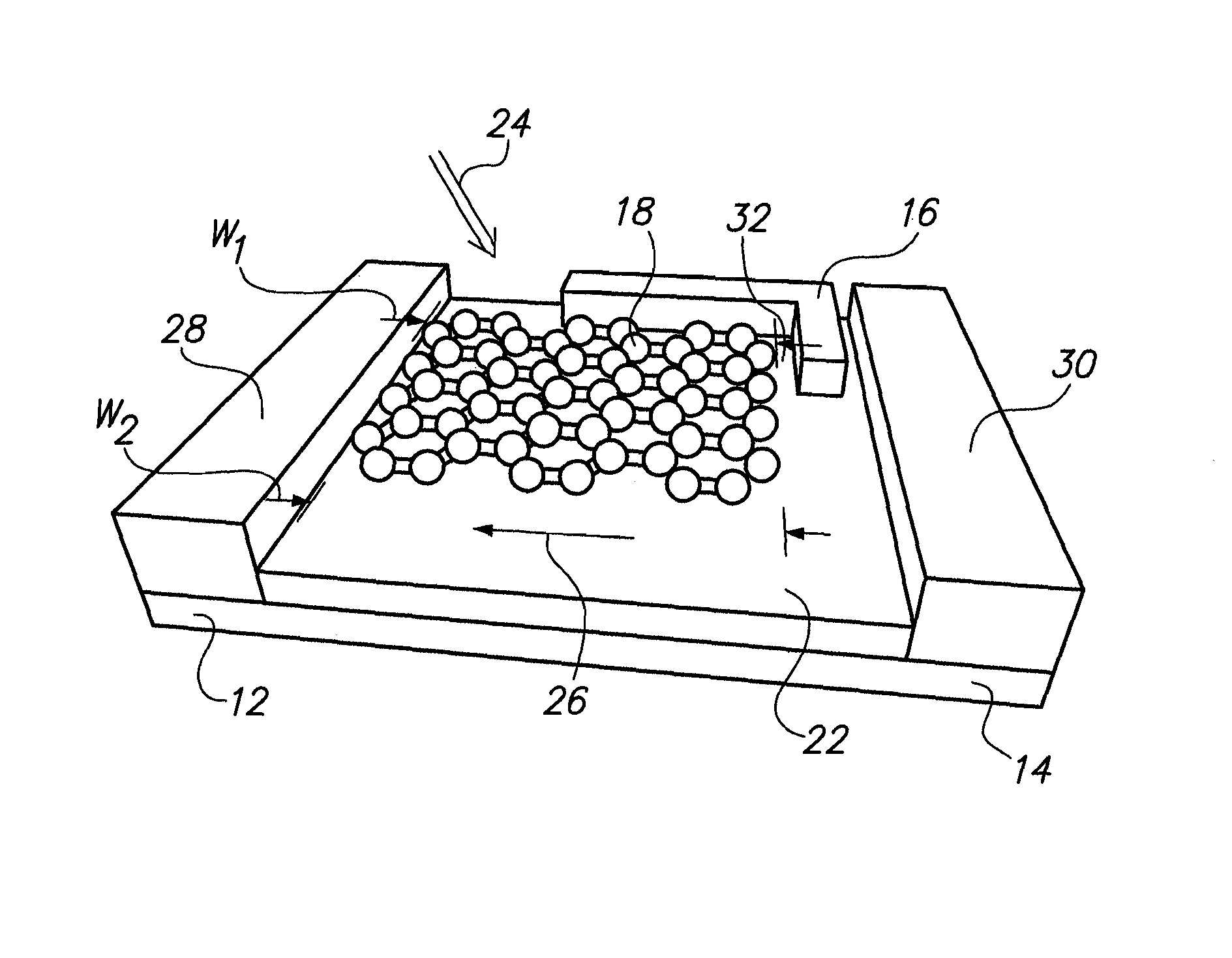
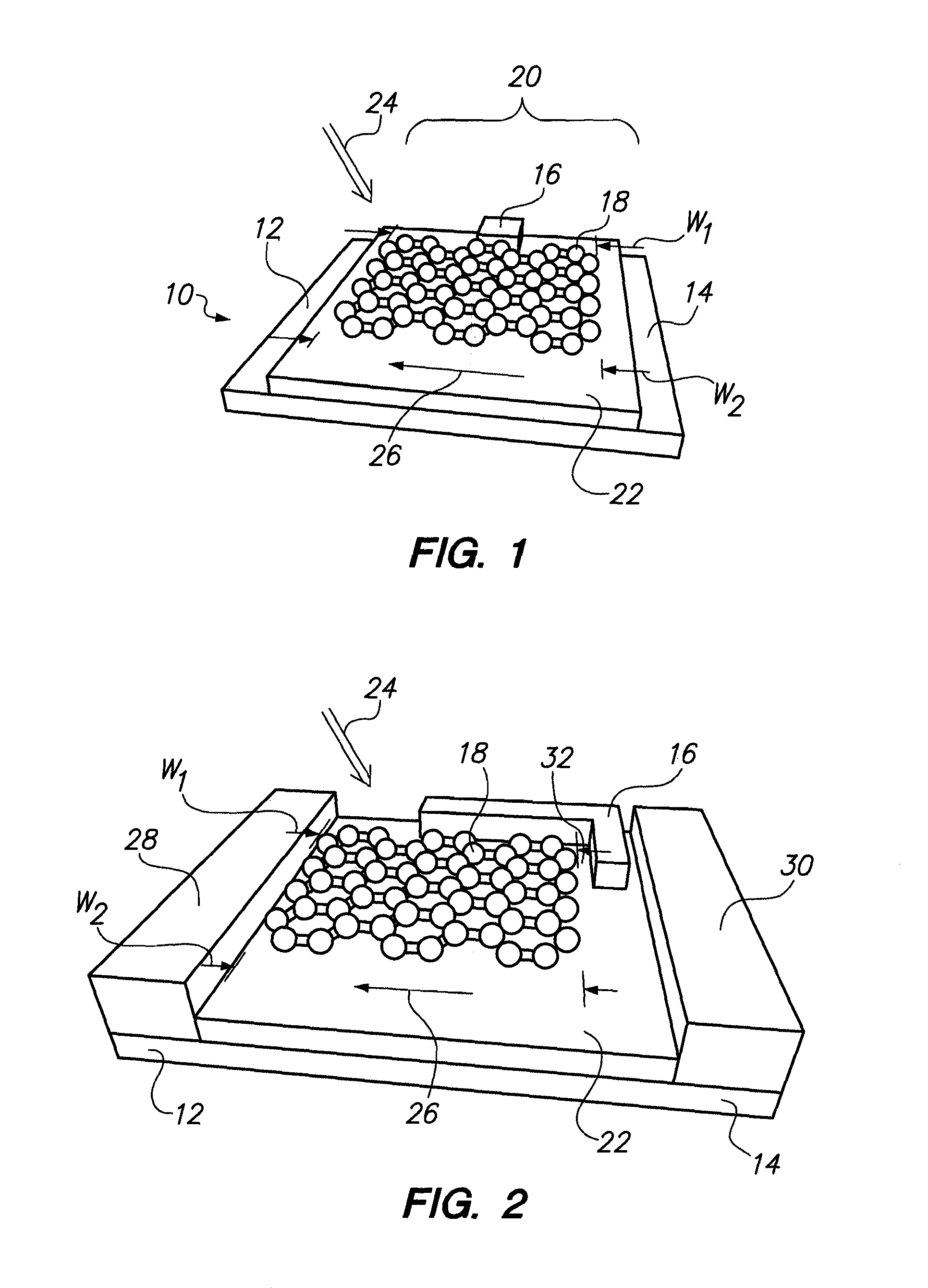
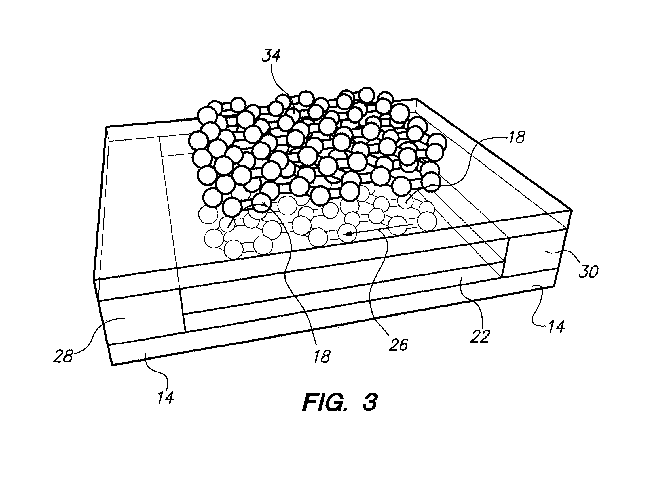
[0014]Referring initially to FIG. 1, a graphene based quantum detector device is shown and is initially designated by reference character 10. As shown, device 10 can be configured in the same manner as a transistor, to include a source 12, a drain 14 and a discharging element 16. A graphene sheet 18 can be included in the device according to several embodiments. Graphene sheet 18 can cooperate with discharging element 16 to function as a gate 20 for the device 10. An insulator layer 22 can separate graphene sheet 18 from source 12 and drain 14.

[0015]The material properties of graphene can allow the structure disclosed herein to function as a transistor using the quantum nature of light. Specifically, due to the zero-bandgap nature of graphene, it can be capable of generating conduction electrons from incident electromagnetic radiation over a wide range of frequencies. As a result, an incident photon will push an electron into the conduction band to create an electron-hole pair. When...


PUM


Abstract

A graphene based detector device can include a source, a drain, and a gate. The gate can incorporate a discharging element and a graphene sheet that is proximate to the discharging element. The graphene sheet for the transistor can have a decreasing width, from a maximum width w2 distal to the discharging element to a minimum width w1 proximate to the discharging element. An electric potential can be established across graphene sheet, to facilitate funneling of the electrons from the graphene sheet (which are caused by quanta of electromagnetic radiation) toward the discharging element. The devices can be formed in an array to establish an antenna that operates according to the quantum nature of light, as opposed to resonance (wavelength). Multiple graphene layers that are doped using different materials can be included. The multiple layer funnel electrons at specific frequencies, to create an operating frequency range for the device.

Description

FEDERALLY-SPONSORED RESEARCH AND DEVELOPMENT[0001]This invention (Navy Case No. 101319) is assigned to the United States Government and is available for licensing for commercial purposes. Licensing and technical inquires may be directed to the Office of Research and Technical Applications, Space and Naval Warfare Systems Center, Pacific, Code 72120, San Diego, Calif. 92152; voice (619) 553-5118; email ssc pac T2@navy.mil.FIELD OF THE INVENTION[0002]The present invention pertains generally to devices that convert quanta of electromagnetic radiation into an electrical signal. More specifically, the present invention pertains to devices that use graphene to convert quanta of electromagnetic radiation over a wide frequency range into a proportional electrical signal.BACKGROUND OF THE INVENTION[0003]Ordinary antennas operate on the concept of resonance. For these antennas, the size of the antenna is directly related to the wavelength of the electromagnetic wave it detects. The resonance ...

Claims


Application Information

Patent Timeline
Patent Type & Authority Patents(United States)
IPC IPC(8): H01L31/028H01L29/16
CPCH01L29/1606H01L31/028H01L31/113H01L29/78684H01L29/78696Y02E10/547
Inventor DE ANDRADE, MARCLO C.LEESE DE ESCOBAR, ANNA M.GARMIRE, DAVIDKAMIN, NACKIEB
Owner THE UNITED STATES OF AMERICA AS REPRESENTED BY THE SECRETARY OF THE NAVY
Why Eureka
Try Eureka