
Semiconductor device and method of manufacturing semiconductor device

a semiconductor and semiconductor technology, applied in the field of semiconductor devices, can solve the problems of short circuit and inability to reduce the leakage current between the source and the drain, and achieve the effect of reducing the leakage curren

Active Publication Date: 2014-09-23
LAPIS SEMICON CO LTD
View PDF4 Cites 3 Cited by
  • Summary
  • Abstract
  • Description
  • Claims
  • Application Information

AI Technical Summary

Benefits of technology

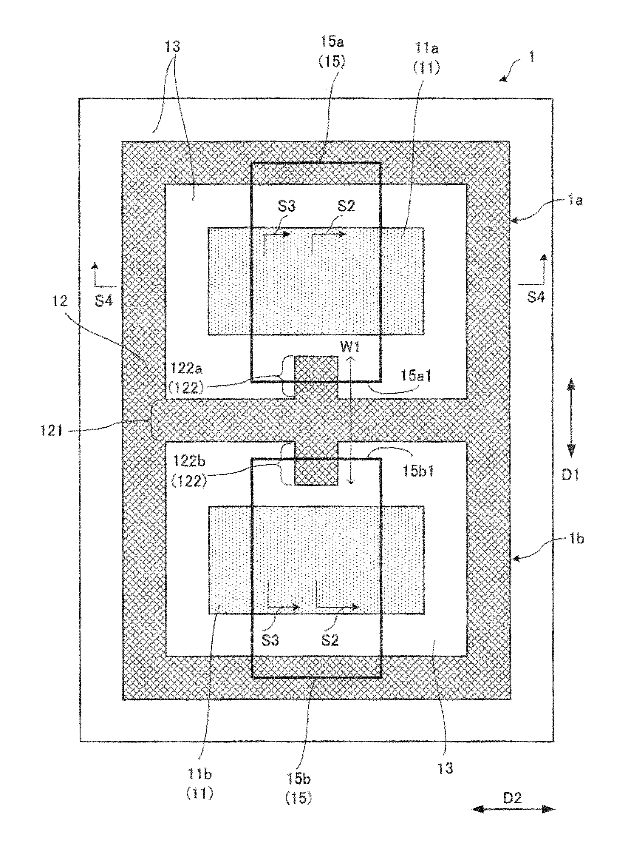
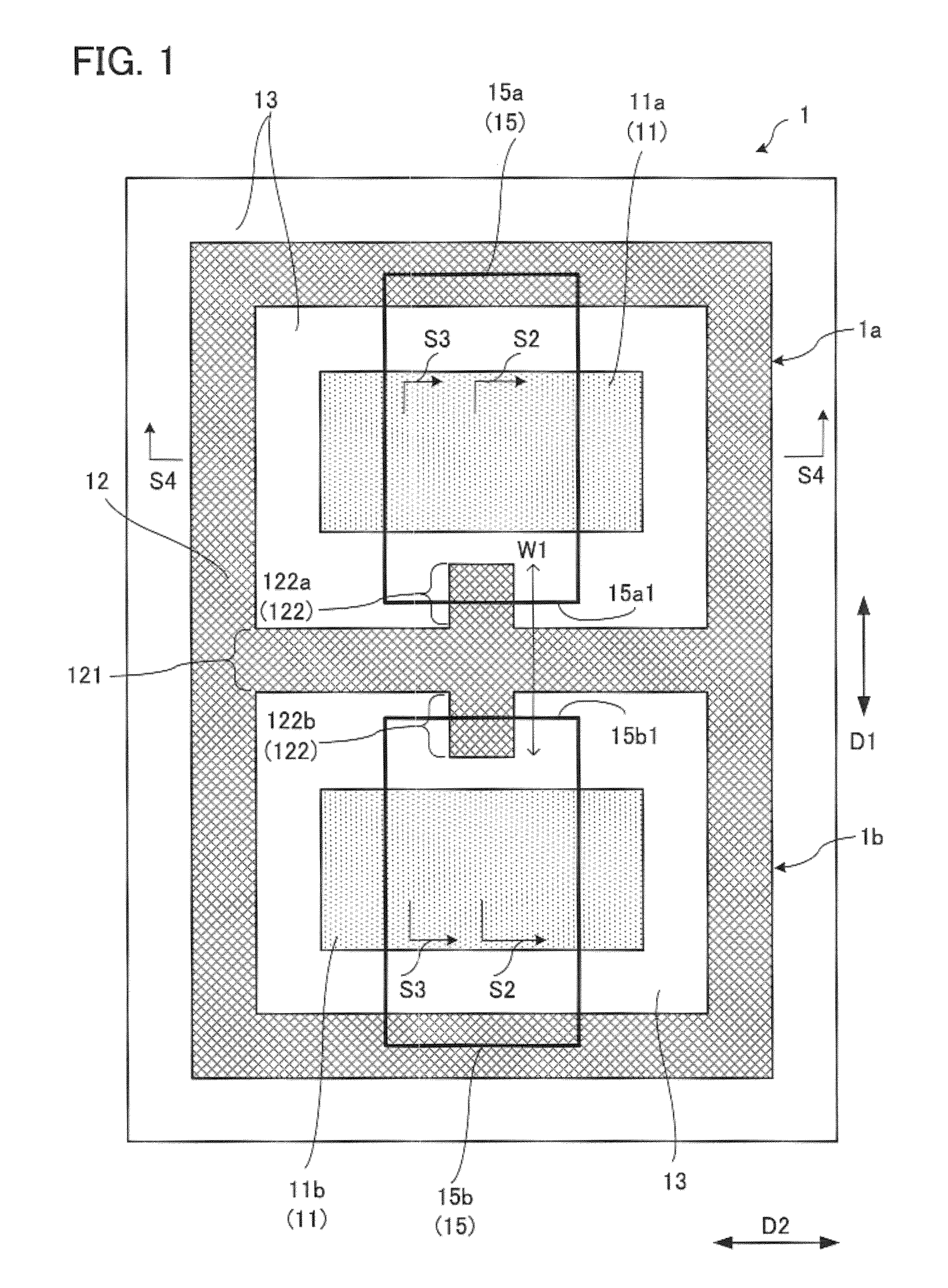
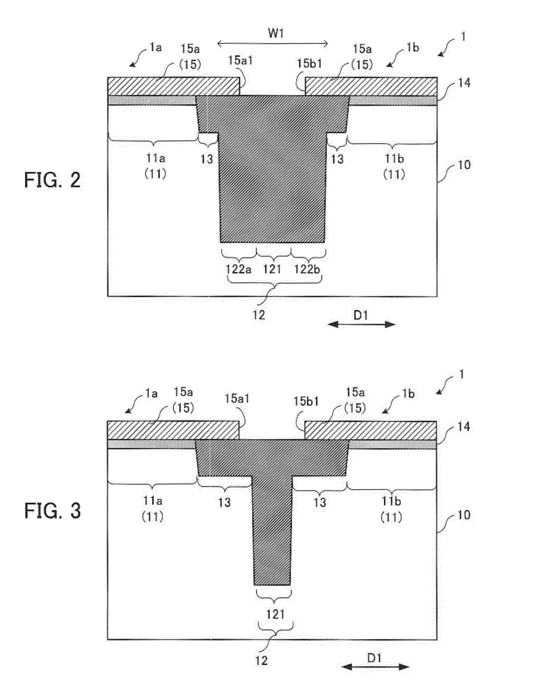
[0006]It is an object of the present invention to provide a semiconductor device capable of reducing a leakage current between a source and a drain and making it difficult to cause a short circuit between adjacent gate electrodes, even if a width of an element isolating region is extremely small in a trench structure, and to provide a method of manufacturing the semiconductor device.
[0009]According to the present invention, it is possible to reduce a leakage current between a source and a drain and moreover, it is possible to make it difficult to cause a short circuit between adjacent gate electrodes.

Problems solved by technology

However, in a case where the element isolating region is formed to have an extremely small width in the trench structure for further improving integration, some problematic states are expected: a state where the edge side of the gate electrode is not placed on the element isolating region due to the manufacturing error of the edge side of the gate electrode and therefore a leakage current between the source and the drain cannot be reduced, a state where adjacent gate electrodes are overlapped each other on the element isolating region with the result that a short circuit occurs between the adjacent gate electrodes, and so on.

Method used


Image

  • Semiconductor device and method of manufacturing semiconductor device
  • Semiconductor device and method of manufacturing semiconductor device
  • Semiconductor device and method of manufacturing semiconductor device

Examples


first embodiment

(1-6) Modified Example of First Embodiment

[0075]FIG. 20 is a plan view schematically illustrating a semiconductor device 2 according to a modified example of the first embodiment. FIG. 21 is a longitudinal cross-sectional view schematically illustrating the semiconductor device 2 taken along a plane indicated by a line S21-S21 in FIG. 20. As illustrated in FIGS. 20 and 21, in the modified example of the first embodiment, the semiconductor device 2 (or 2a, 2b) has a semiconductor substrate 20, active regions 21 (or 21a, 21b), a first element isolating region 22 which is a DTI region 22 (or 221, 222; or 221, 222a, 222b), gate insulating films 24 (or 24a, 24b), and gate electrodes 25 (or 25a, 25b). The semiconductor device 2 differs from the semiconductor device 1 of the first embodiment in a point that the semiconductor device 2 illustrated in FIGS. 20 and 21 does not have the second element isolating region 13.

[0076]As illustrated in FIG. 20 or 21, the plurality of active regions 21 ...

second embodiment

(2-3) Modified Example of Second Embodiment

[0092]FIG. 28 is a plan view schematically illustrating a semiconductor device 4 according to a modified example of the second embodiment. FIG. 29 is a longitudinal cross-sectional view schematically illustrating the semiconductor device 4 taken along a plane indicated by a line S29-S29 in FIG. 28. As illustrated in FIGS. 28 and 29, the semiconductor device 4 (or 4a, 4b) according to the modified example of the second embodiment has a semiconductor substrate 40, active regions 41 (or 41a, 41b), a first element isolating region 42 (or 421, 422; or 421, 422a, 422b) which is a DTI region, gate insulating films 44 (or 44a, 44b), and gate electrodes 45 (or 45a, 45b). The semiconductor device 4 illustrated in FIGS. 28 and 29 does not have the second element isolating region 33, and the semiconductor device 4 differs from the semiconductor device 3 according to the second embodiment in this point.

[0093]As illustrated in FIG. 28 or 29, the pluralit...

third embodiment

(3-3) Modified Example of Third Embodiment

[0109]FIG. 36 is a plan view schematically illustrating a semiconductor device 6 according to a modified example of the third embodiment. FIG. 37 is a longitudinal cross-sectional view schematically illustrating the semiconductor device 6 taken along a plane indicated by a line S37-S37 in FIG. 36. As illustrated in FIGS. 36 and 37, the semiconductor device 6 (or 6a, 6b) according to the modified example of the third embodiment has a semiconductor substrate 60, active regions 61 (or 61a, 61b), a first element isolating region 62 (or 621, 622; or 621a, 621b, 622) which is a DTI region, gate insulating films 64 (or 64a, 64b), and gate electrodes 65 (or 65a, 65b). The semiconductor device 6 illustrated in FIGS. 36 and 37 does not have the second element isolating region 53, and the semiconductor device 6 differs from the semiconductor device 5 in the third embodiment in this point.

[0110]As illustrated in FIG. 36 or 37, the plurality of active re...


PUM


Abstract

Provided is a semiconductor device including active regions formed in a semiconductor substrate and arranged in a first direction parallel to a surface of the semiconductor substrate; a first element isolating region formed in the semiconductor substrate and electrically isolating adjacent active regions from each other; and gate electrodes extending over the active regions respectively and arranged in the first direction. The first element isolating region includes a first region extending in a second direction orthogonal to the first direction and a second region extending in a direction intersecting the first region, one gate electrode of adjacent gate electrodes has a first edge side which includes a first overlap part placed on the second region, and another gate electrode of the adjacent gate electrodes has a second edge side which faces the first edge side and includes a second overlap part placed on the second region.

Description

BACKGROUND OF THE INVENTION[0001]1. Field of the Invention[0002]The present invention relates to a semiconductor device having an element isolating region and a method of manufacturing the semiconductor device.[0003]2. Description of the Related Art[0004]For the purpose of improving integration of a semiconductor integrated circuit or the like, a trench structure has been used as an element isolating region for electrically isolating a plurality of element regions from each other on a semiconductor substrate, as described in Japanese Patent Application Publication No. 10-56059 (Patent Document 1), for example. Besides, it has been known that a leakage current between a source and a drain in a MOS transistor is reduced by forming a gate electrode so that an edge side of the gate electrode is placed on the element isolating region, as described in Japanese Patent Application Publication No. 2010-40896 (Patent Document 2), for example.[0005]However, in a case where the element isolatin...

Claims


Application Information

Patent Timeline
Patent Type & Authority Patents(United States)
IPC IPC(8): H01L27/088H01L29/78H01L29/66H01L27/02H01L21/8234
CPCH01L29/66484H01L29/0692H01L27/0207H01L27/088H01L21/823437H01L21/823481H01L29/7831H01L21/76232
Inventor KAMOSHITA, JUNICHI
Owner LAPIS SEMICON CO LTD
Learn More