Electronic component mounting method providing a substrate standby area

a technology for electronic components and standby areas, which is applied in the direction of transportation and packaging, manufacturing tools, conveyers, etc., can solve the problems of difficult to provide an electronic component mounting system having a compact facility, and achieve the effects of compact facility, enhanced production efficiency, and eliminated waste of tim

Active Publication Date: 2014-07-29
PANASONIC CORP
View PDF15 Cites 2 Cited by
  • Summary
  • Abstract
  • Description
  • Claims
  • Application Information

AI Technical Summary

Benefits of technology

[0005]An object of the invention is to provide an electronic component mounting system and an electronic component mounting method for eliminating the waste of time attributable to transfer of substrates and enhancing the production efficiency by a compact facility.
[0008]According to the invention, while a plurality of electronic component mounting apparatuses are coupled in series, a substrate carried into a work conveyor is temporarily placed in a standby state in a substrate standby area formed by the carry-in conveyor of one electronic component mounting apparatus and the carry-out conveyor of another electronic component mounting apparatus positioned upstream of the one electronic component mounting apparatus. This eliminates the waste of time attributable to transfer of substrates and enhances the production efficiency by a compact facility.

Problems solved by technology

Thus, in the related art, it has been difficult to provide an electronic component mounting system having a compact facility that eliminates the waste of time attributable to transfer of substrates.

Method used


Image

  • Electronic component mounting method providing a substrate standby area
  • Electronic component mounting method providing a substrate standby area
  • Electronic component mounting method providing a substrate standby area

Examples


Embodiment Construction

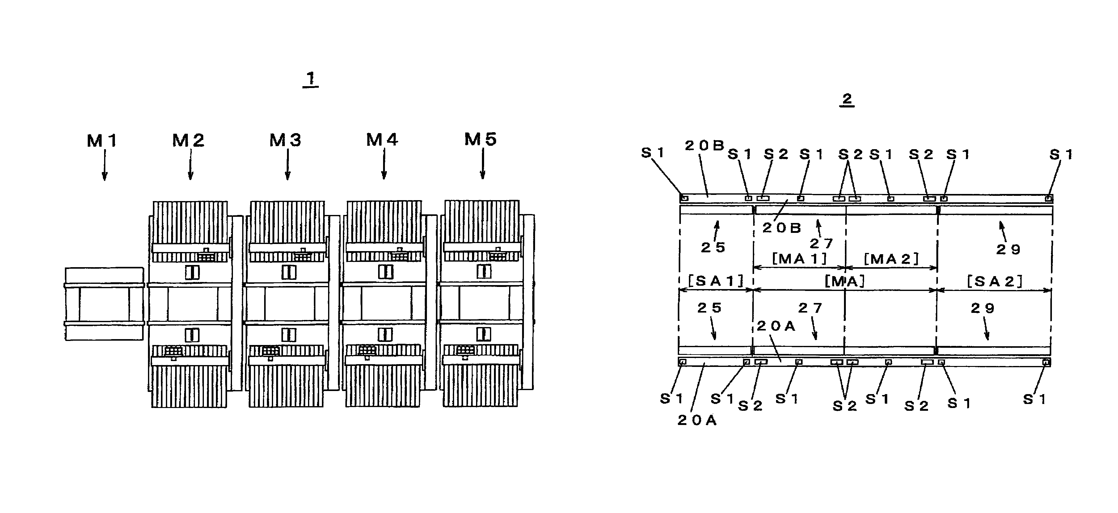
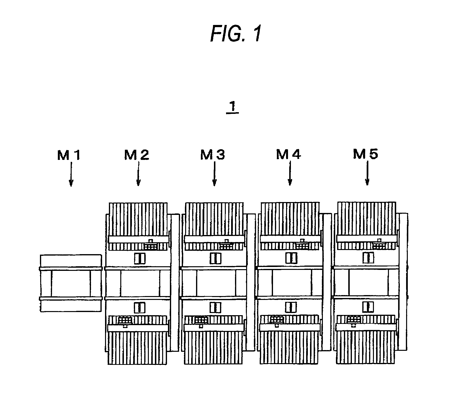
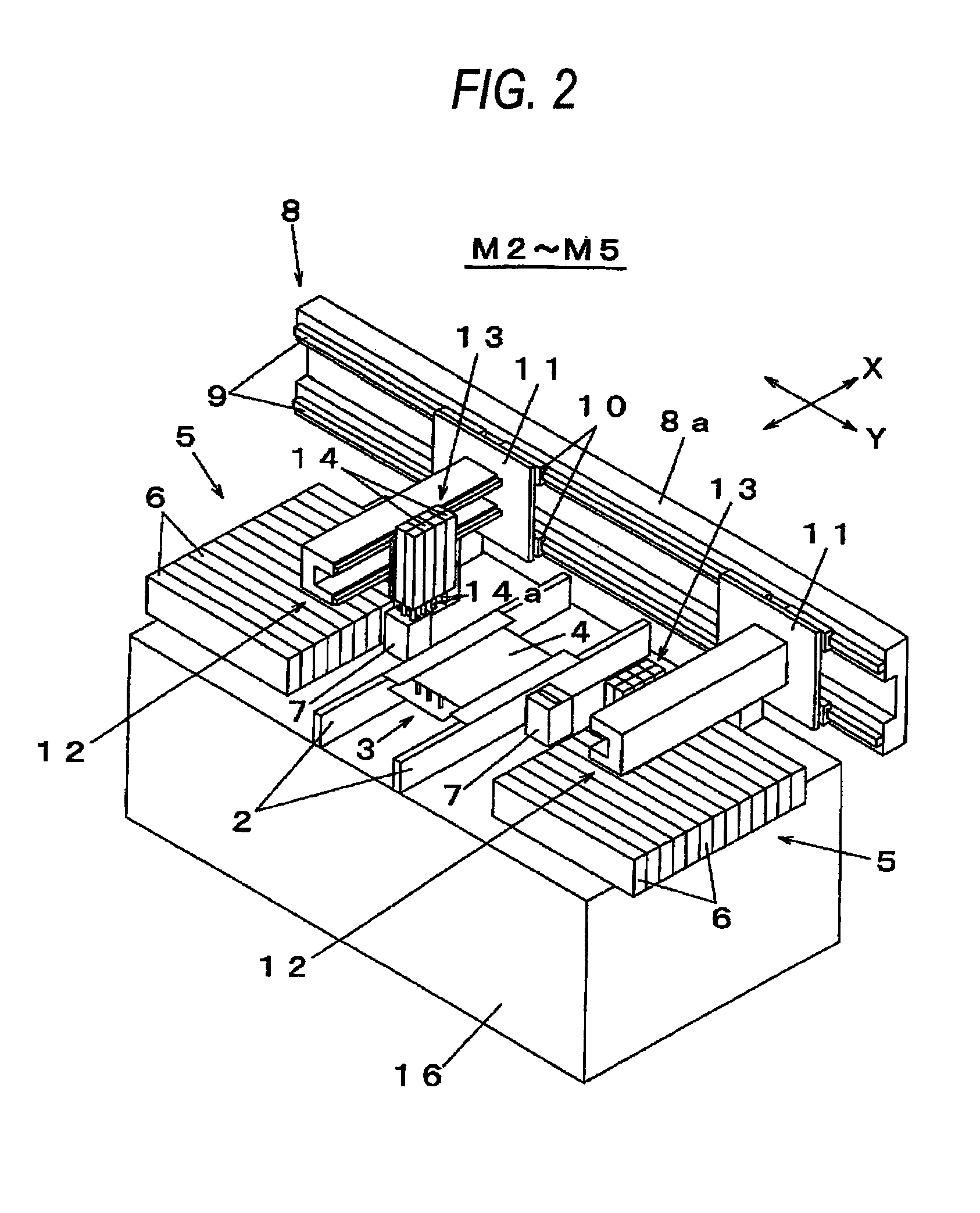
[0018]Next, an embodiment of the invention will be described referring to figures. FIG. 1 illustrates the configuration of an electronic component mounting system according to an embodiment of the invention. FIG. 2 is a perspective view of an electronic component mounting apparatus of the electronic component mounting system according to the embodiment of the invention. FIG. 3 is a plan view of an electronic component mounting apparatus of the electronic component mounting system according to the embodiment of the invention. FIGS. 4A and 4B illustrate the structure of a substrate transfer mechanism in an electronic component mounting apparatus of the electronic component mounting system according to the embodiment of the invention. FIG. 5 is a partial cross-sectional view of an electronic component mounting apparatus of the electronic component mounting system according to the embodiment of the invention. FIGS. 6A and 6B illustrate a mounting area, a standby area and a sensor arrang...


PUM

PropertyMeasurementUnit
standby areaaaaaaaaaaa
areaaaaaaaaaaa
sizeaaaaaaaaaa

Abstract

In an electronic component mounting system including a plurality of electronic component mounting apparatuses coupled in series, the system mounting an electronic component on a substrate to manufacture a mounted substrate, a substrate carried into a mounting conveyor is temporarily placed in a standby state in a substrate standby area formed by a first transfer conveyor (carry-in conveyor) of one electronic component mounting apparatus and a second transfer conveyor (carry-out conveyor) of another electronic component mounting apparatus positioned upstream of the one electronic component mounting apparatus.

Description

BACKGROUND OF THE INVENTION[0001]The present invention relates to an electronic component mounting system and an electronic component mounting method for mounting an electronic component on a substrate.RELATED ART[0002]An electronic component mounting system for mounting an electronic component on a substrate is composed of a plurality of electronic component mounting apparatuses coupled to each other. An electronic component mounting apparatus includes a substrate transfer mechanism for horizontally transferring a substrate. Electronic components are sequentially mounted on a target substrate as each electronic component mounting apparatus is being moved from upstream to downstream by the substrate transfer mechanism. As a substrate transfer mechanism, a belt-conveyor type substrate transfer mechanism is often used (for example, refer to Japanese Patent JP-3671681).[0003]In order to enhance the efficiency of work by an electronic component mounting system, it is necessary to minimi...

Claims


Application Information

Patent Timeline
Patent Type & Authority Patents(United States)
IPC IPC(8): B23P19/00
CPCY10T29/53187Y10T29/53183Y10T29/4913Y10T29/53178H05K13/0452H05K13/0069Y10T29/49131H05K13/0061H05K13/0495H01L21/52H01L21/67144H01L21/67706H01L21/67721H01L21/67736
Inventor YAGI, SHUZONAKANE, MASAOFURUTA, NOBORU
Owner PANASONIC CORP
Why Eureka
Try Eureka