
Wavelength-converting light emitting diode (LED) chip and LED device equipped with chip

a light-emitting diode and wavelength-converting technology, which is applied in the manufacture of semiconductor/solid-state devices, semiconductor devices, electrical appliances, etc., can solve the problems of phosphors having a low reproduction rate, light-emitting efficiency deterioration and hue deviation by far field beam distribution, etc., and achieve the effect of optimizing the color conversion efficiency of white ligh

Inactive Publication Date: 2014-03-25
SAMSUNG ELECTRONICS CO LTD
View PDF34 Cites 5 Cited by
  • Summary
  • Abstract
  • Description
  • Claims
  • Application Information

AI Technical Summary

Benefits of technology

The invention provides a solution for addressing issues with non-uniform distribution of phosphors and color reproduction in LED chips. By adding a phosphor layer on top of the LED chip, with a dome-like convex meniscus shape, the phosphor layer can be controlled to improve far field beam distribution and hue deviation. This results in improved color conversion efficiency and CRI (measuring the accuracy of color reproduction) using a double-layered structure.

Problems solved by technology

That is, when the phosphors are not uniformly distributed inside a resin encasing portion, light emitting efficiency deterioration and hue deviation by far field beam distribution may occur.
In addition, when two or more kinds of phosphors (for example, a combination selected from yellow, green, an red phosphors) are used to improve a color rendering index (CRI), a problem due to the non-uniform distribution of phosphors may become more serious.
More particularly, in a light emitting device having a high flux LED driven by a high current, the distribution of irregular phosphors having a low reproduction rate has the disadvantage of accelerating the color conversion efficiency reduction rate and the reliability reduction rate to an even greater degree.

Method used


Image

  • Wavelength-converting light emitting diode (LED) chip and LED device equipped with chip
  • Wavelength-converting light emitting diode (LED) chip and LED device equipped with chip
  • Wavelength-converting light emitting diode (LED) chip and LED device equipped with chip

Examples


Embodiment Construction

[0043]The above and other aspects, features and other advantages of the present invention will be more clearly understood from the following detailed description taken in conjunction with the accompanying drawings.

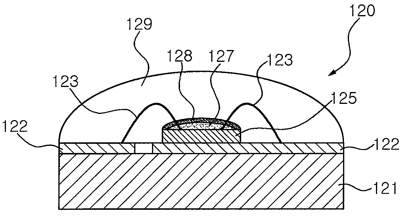
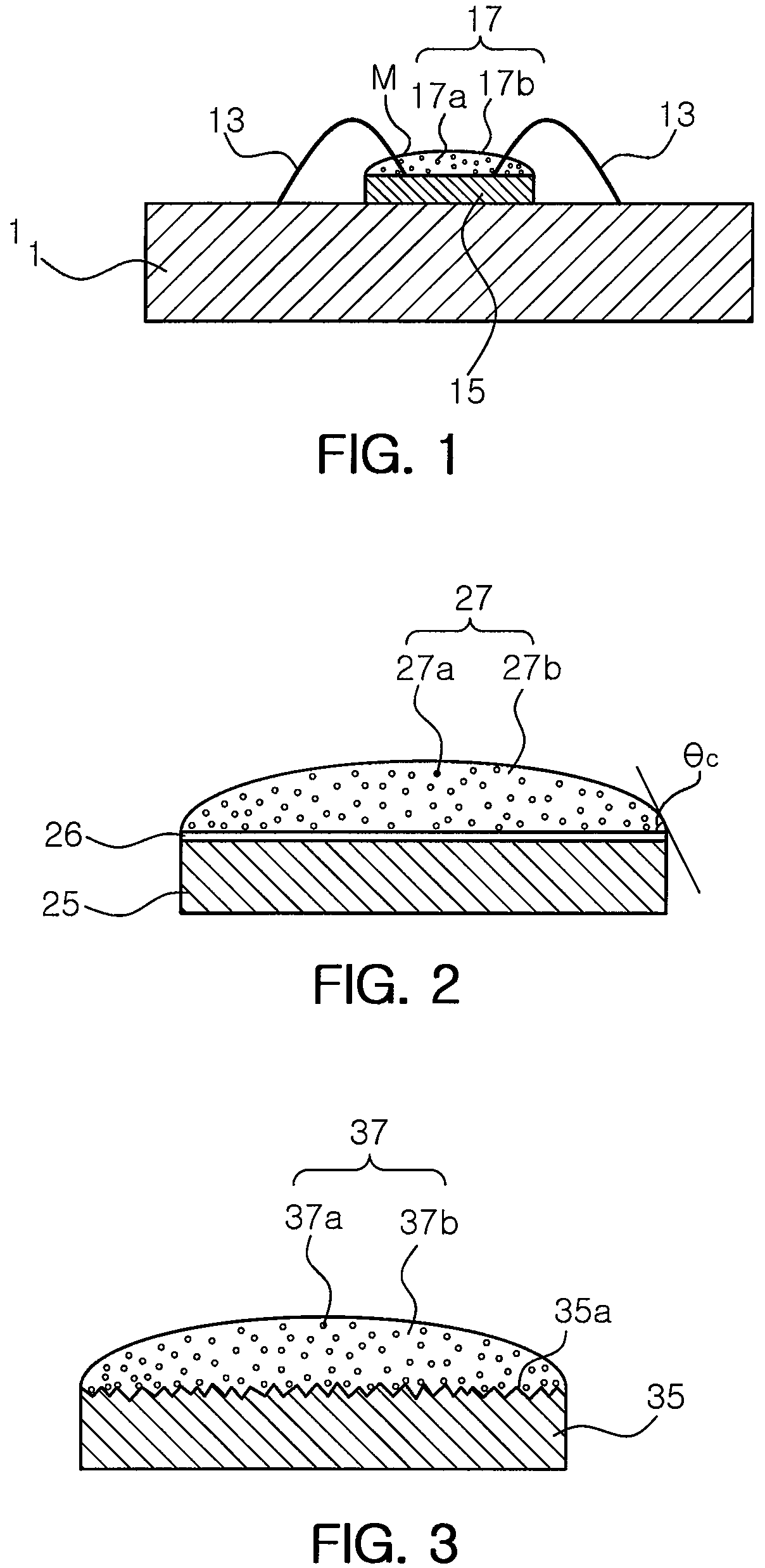
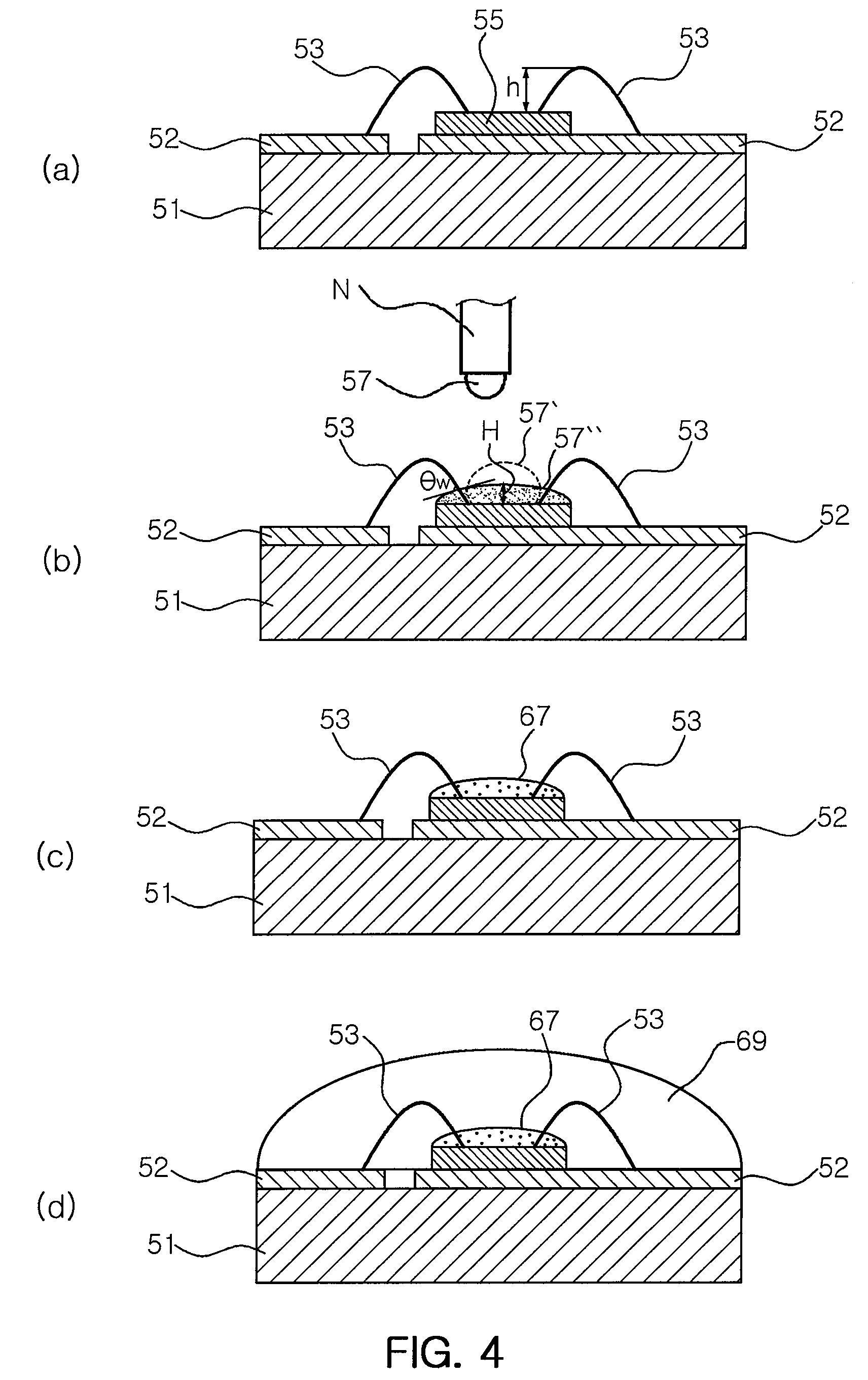
[0044]FIG. 1 is a schematic cross-sectional view illustrating a wavelength-converted light emitting device 10 according to an exemplary embodiment of the present invention.

[0045]Referring to FIG. 1, the wavelength-converted light emitting device 10 includes a substrate 11 which is a member for mounting, and an LED chip 15 mounted on the substrate 11.

[0046]In an exemplary embodiment of the present invention, the LED chip 15 may be fixed on the substrate using an additive member (not shown), and may be electrically connected with lead structures (not shown) of the substrate 11 using wires 13.

[0047]A phosphor layer 17 having a convex meniscus-shaped upper surface M is formed on the upper surface of the LED chip 15. The phosphor layer 17 is formed of a resin 17b containing pho...


PUM


Abstract

A wavelength-converted light emitting diode (LED) chip is provided. The wavelength-converted LED chip includes an LED chip and a wavelength-converted layer. The LED chip emits light in a predetermined wavelength region. The wavelength-converted layer is formed of a resin containing phosphor bodies of at least one kind which convert a portion of the light emitted from the LED chip into light in a different wavelength region. The wavelength-converted layer is formed on an upper surface of the LED chip, and has a convex meniscus-shaped upper surface.

Description

RELATED APPLICATIONS[0001]This application is the U.S. National Phase under 35 U.S.C. §371 of International Application No. PCT / KR2009 / 003647, filed on Jul. 3, 2009, which in turn claims the benefit of Korean Application No. 10-2008-0064381, filed on Jul. 3, 2008, Korean Application No. 10-2008-0085556, filed on Aug. 29, 2008 and Korean Application No. 10-2009-0060596, filed Jul. 3, 2009 the disclosures of which Applications are incorporated by reference herein.TECHNICAL FIELD[0002]The present invention relates to a wavelength-converted light emitting diode (LED) chip, and more particularly, to a wavelength-converted LED chip that can emit white light by mixing original light emitted from the LED chip with secondary light from at least one phosphor excited by a portion of the original light emission, and a wavelength-converted light emitting device having the same.BACKGROUND ART[0003]A semiconductor LED is known as a next generation light source having the advantages of a long life ...

Claims


Application Information

Patent Timeline
Patent Type & Authority Patents(United States)
IPC IPC(8): H01L31/0232
CPCH01L33/508H01L2933/0091H01L33/504H01L33/502H01L33/505H01L33/54H01L33/56H01L33/58H01L2224/48091H01L2224/8592H01L2224/45139H01L2924/181H01L2924/00014H01L2924/00011H01L2924/00012H01L2224/45015H01L2924/207H01L2924/01049H01L2924/00
Inventor KIM, YONG TAELEE, DONG YEOUL
Owner SAMSUNG ELECTRONICS CO LTD
Learn More