
System and methods for extracting correlation curves for an organic light emitting device

a light emitting device and correlation curve technology, applied in the field of displays, can solve the problems of light output at a constant current to decrease, current to drop at a constant bias voltage, and oled device also undergoes electrical degradation

Active Publication Date: 2013-11-19
IGNIS INNOVATION
View PDF46 Cites 23 Cited by
  • Summary
  • Abstract
  • Description
  • Claims
  • Application Information

AI Technical Summary

Problems solved by technology

During operation of an organic light emitting diode device, it undergoes degradation, which causes light output at a constant current to decrease over time.
The OLED device also undergoes an electrical degradation, which causes the current to drop at a constant bias voltage over time.
These degradations are caused primarily by stress related to the magnitude and duration of the applied voltage on the OLED and the resulting current passing through the device.
However, the optical aging effect of the OLED is dependent on the stress conditions placed on individual pixels as well, and since the stresses vary from pixel to pixel, accurate compensation is not assured unless the compensation tailored for a specific stress level is determined.

Method used


Image

  • System and methods for extracting correlation curves for an organic light emitting device
  • System and methods for extracting correlation curves for an organic light emitting device
  • System and methods for extracting correlation curves for an organic light emitting device

Examples


Embodiment Construction

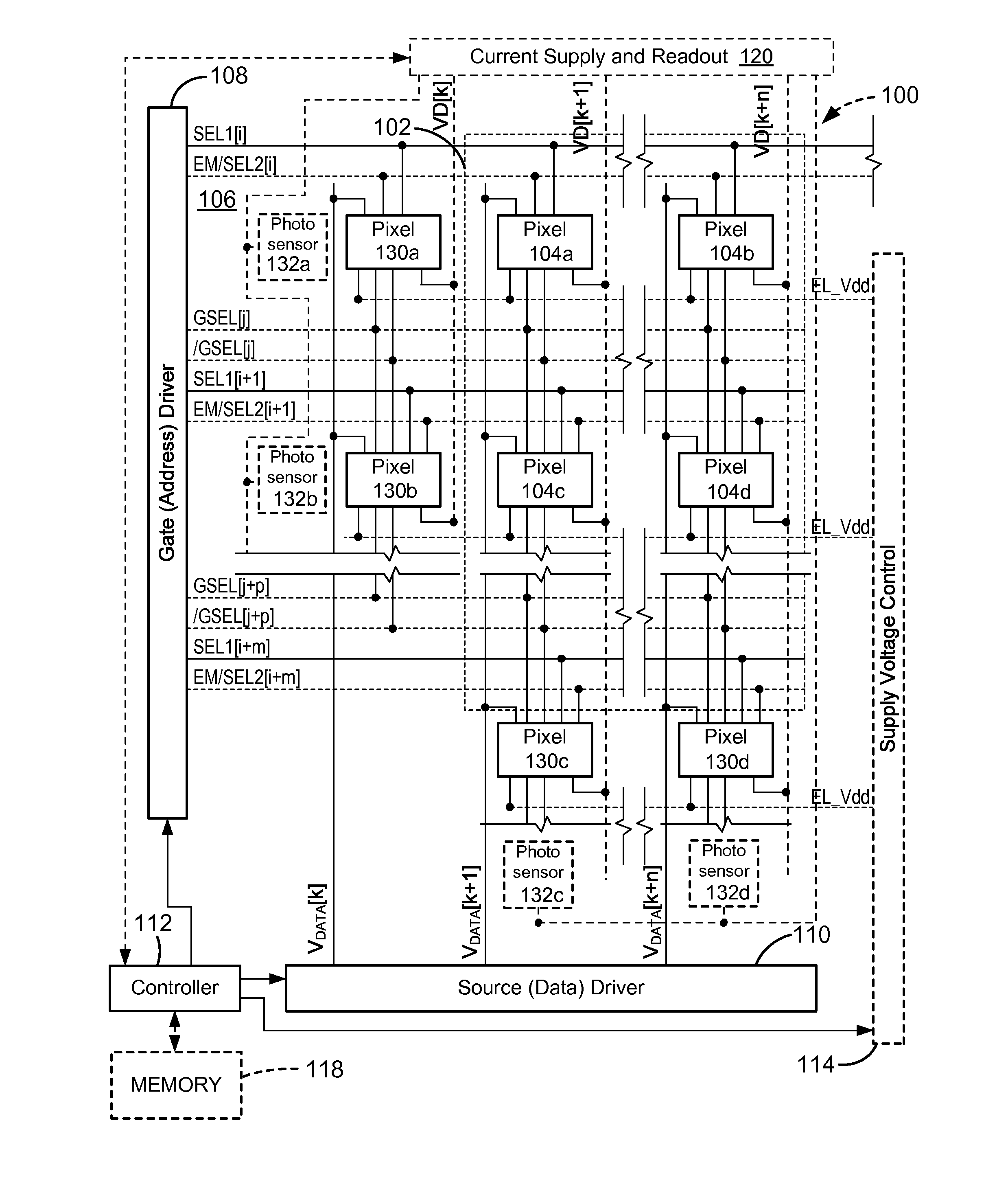
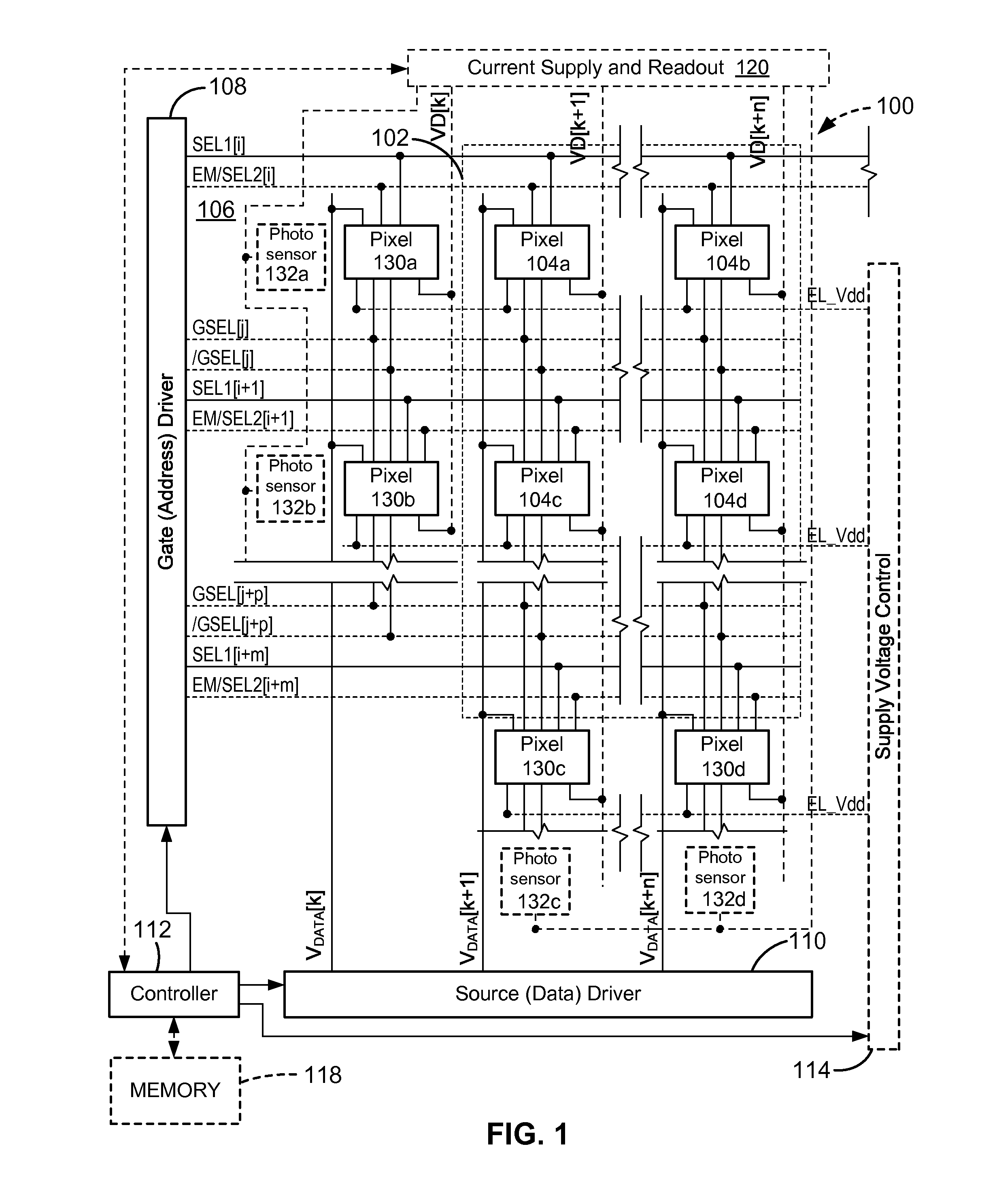
[0021]FIG. 1 is an electronic display system 100 having an active matrix area or pixel array 102 in which an array of active pixels 104a-104d are arranged in a row and column configuration. For ease of illustration, only two rows and columns are shown. External to the active matrix area, which is the pixel array 102, is a peripheral area 106 where peripheral circuitry for driving and controlling the area of the pixel array 102 are disposed. The peripheral circuitry includes a gate or address driver circuit 108, a source or data driver circuit 110, a controller 112, and an optional supply voltage (e.g., EL_Vdd) driver 114. The controller 112 controls the gate, source, and supply voltage drivers 108, 110, 114. The gate driver 108, under control of the controller 112, operates on address or select lines SEL[i], SEL[i+1], and so forth, one for each row of pixels 104a-104b and 104c-104d in the pixel array 102. In pixel sharing configurations described below, the gate or address driver ci...


PUM


Abstract

A system and method for determining and applying characterization correlation curves for aging effects on an organic light organic light emitting device (OLED) based pixel is disclosed. A first stress condition is applied to a reference pixel having a drive transistor and an OLED. An output voltage based on a reference current is measured periodically to determine an electrical characteristic of the reference pixel under the first predetermined stress condition. The luminance of the reference pixel is measured periodically to determine an optical characteristic of the reference pixel. A characterization correlation curve corresponding to the first stress condition including the determined electrical and optical characteristic of the reference pixel is stored. The stress condition of an active pixel is determined and a compensation voltage is determined by correlating the stress condition of the active pixel with the curves of the predetermined stress conditions.

Description

CROSS-REFERENCE TO RELATED APPLICATIONS[0001]This application claims priority to Canadian Application No. 2,692,097, which was filed Feb. 4, 2010.FIELD OF THE INVENTION[0002]This invention is directed generally to displays that use light emissive devices such as OLEDs and, more particularly, to extracting characterization correlation curves under different stress conditions in such displays to compensate for aging of the light emissive devices.BACKGROUND OF THE INVENTION[0003]Currently, active matrix organic light emitting device (“AMOLED”) displays are being introduced for numerous applications. The advantages of such displays include lower power consumption, manufacturing flexibility, and faster refresh rate over conventional liquid crystal displays. In contrast to conventional liquid crystal displays, there is no backlighting in an AMOLED display as each pixel consists of different colored OLEDs emitting light independently. The OLEDs emit light based on current supplied through ...

Claims


Application Information

Patent Timeline
Patent Type & Authority Patents(United States)
IPC IPC(8): G01R19/00G01R21/133G01R19/25G09G3/3208
CPCG09G3/32G09G3/006G09G3/3258G09G2320/043G09G3/3291G09G2300/0413G09G2320/0285G09G2320/029G09G2360/145G09G2320/045
Inventor CHAJI, GHOLAMREZAJAFFARI, JAVIDNATHAN, AROKIA
Owner IGNIS INNOVATION
Learn More