Solid-state imaging device
a solid-state imaging and imaging device technology, applied in the direction of semiconductor devices, basic electric elements, electrical apparatus, etc., can solve the problems of deteriorating condensing efficiency of light guides, and achieve the effect of improving condensing efficiency and reducing reflection
- Summary
- Abstract
- Description
- Claims
- Application Information
AI Technical Summary
Benefits of technology
Problems solved by technology
Method used
Image
Examples
embodiment 1
[0038
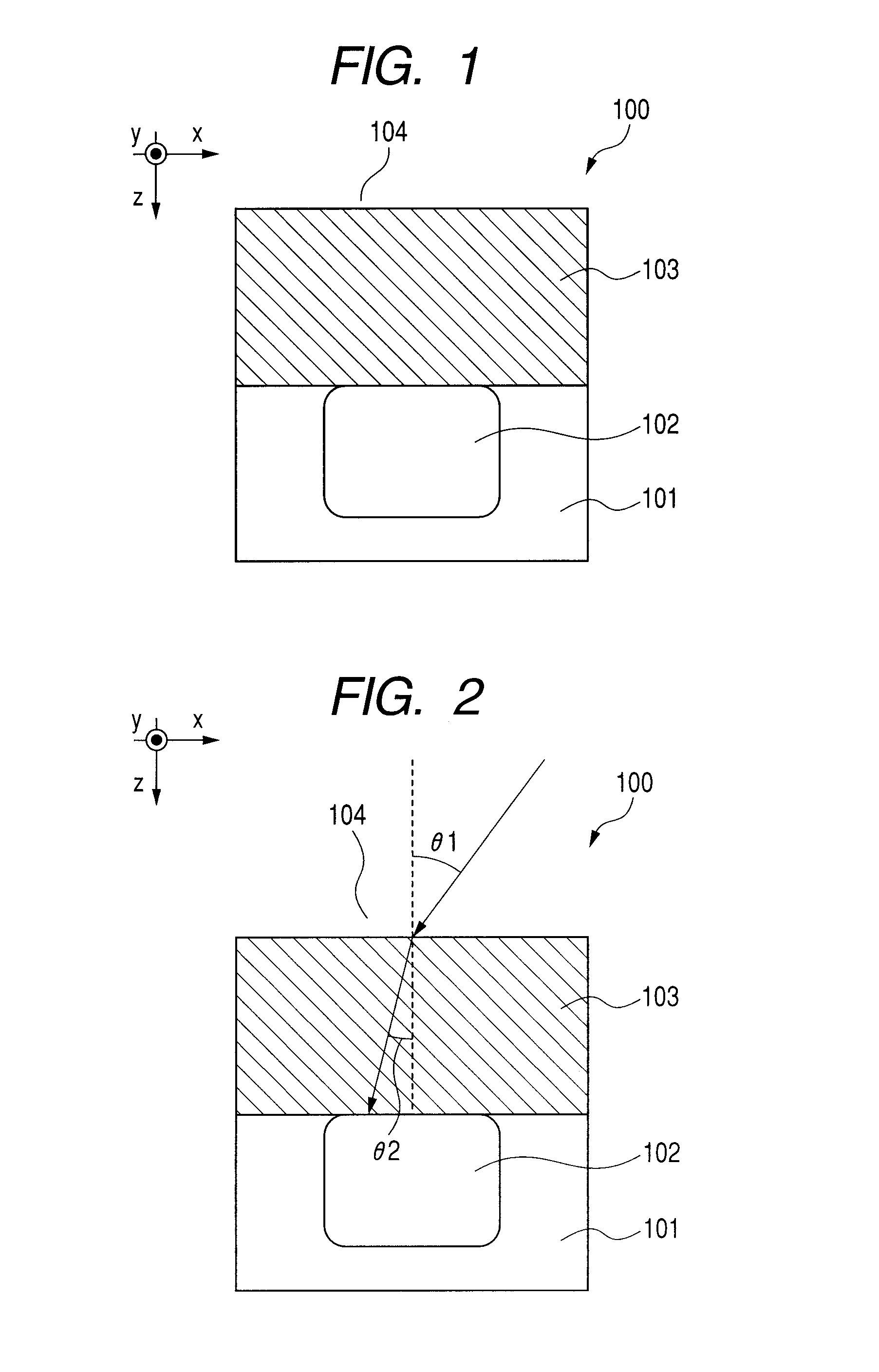
[0039]An example of a solid-state imaging device according to an embodiment 1 of the present invention will be described using FIG. 1. FIG. 1 illustrates a schematic sectional view of a pixel unit 100 of the solid-state imaging device. The solid-state imaging device includes a substrate internally containing a photoelectric conversion unit of this embodiment, and a condensing unit provided on an optical incident side of the substrate. Incident light from the optical incident side is guided through the condensing unit to the photoelectric conversion unit. The solid-state imaging device of this embodiment includes a plurality of pixel units 100 arranged in a matrix manner. The pixel unit 100 includes a silicon substrate 101 and a photoelectric conversion unit 102 arranged inside of the silicon substrate 101. In the pixel unit 100, a condensing unit 103 is formed above the silicon substrate 101. Hereinafter, a region above the condensing unit 103 is referred to as an optical incid...
embodiment 2
[0058
[0059]A solid-state imaging device according to an embodiment 2 will be described using FIGS. 8A and 8B. This embodiment is different from the embodiment 1 in the following configuration. That is, in this embodiment, the specific permittivity ∈ and the specific permeability μ of the condensing unit 113 satisfy the expression of condition, |N1|102 is N3, the value of √∈ / √μ is changed so as to hold √∈ / √μ=N1 at the optical incident side and √∈ / √μ=N3 at the photoelectric conversion unit side.
[0060]As described above, the smaller the reflectivity on the boundary interface is, the closer to one the impedance ratio between two media contact with each other at the boundary becomes. Accordingly, if √∈ / √μ=N3 holds, the reflection between the condensing unit 113 and the photoelectric conversion unit 102 can be suppressed. Further, the absolute value |√∈×√μ| of the refractive index of the condensing unit 113 has a value higher than the absolute value |N1| of the refractive index of the opt...
embodiment 3
[0065
[0066]An example of a configuration of a solid-state imaging device according to an embodiment 3 will be described using FIGS. 9A and 9B. This embodiment is different from the embodiment 1 in the following configuration. That is, this embodiment includes a structure where a barrier unit 105 is arranged around the condensing unit 103, as illustrated in FIG. 9A. Further, provided that the specific permittivity of the barrier unit 105 is ∈2 and the specific permeability is μ2, the barrier unit 105 is configured so as to satisfy the following relationship (Expression 3).
|√∈2×√μ2|<|√∈×√μ| (Expression 3)
[0067]If the absolute value |√∈×√μ| of the refractive index of the condensing unit 103 is larger than the absolute value |√∈2×√μ2| of the refractive index of the barrier unit 105, the light incident from the optical incident unit 104 can be condensed in the condensing unit 103 and guided to the photoelectric conversion unit 102. Accordingly, light leaking to adjacent pixels can be re...
PUM
 Abstract
Description
Claims
Application Information
 - R&D
- Intellectual Property
- Life Sciences
- Materials
- Tech Scout
- Unparalleled Data Quality
- Higher Quality Content
- 60% Fewer Hallucinations
Browse by: Latest US Patents, China's latest patents, Technical Efficacy Thesaurus, Application Domain, Technology Topic, Popular Technical Reports.
© 2025 PatSnap. All rights reserved.Legal|Privacy policy|Modern Slavery Act Transparency Statement|Sitemap|About US| Contact US: help@patsnap.com


