
High output small area group III nitride LEDs

a light-emitting diode, small area technology, applied in the direction of semiconductor devices, basic electric elements, electrical appliances, etc., can solve the problems of unimportant or specifically undesired visual appearance to the human eye, historically more difficult to produce and work wide bandgap semiconductors, and difficult or impossible to grow from melts. , to achieve the effect of low forward voltage, high light output and small siz

Active Publication Date: 2013-08-20
CREELED INC
View PDF78 Cites 13 Cited by
  • Summary
  • Abstract
  • Description
  • Claims
  • Application Information

AI Technical Summary

Benefits of technology

The technical effect of this patent is that it describes an LED (light-emitting diode) with several benefits: It's tiny, requires less electricity than other similar devices, and produces more light compared to its size.

Problems solved by technology

This patent describes improving the performance of small-size LEDs made from group III nitrides grown on silicon carriers. The technical problem addressed is how to increase the output of these LEDs while maintaining their compactness and minimizing damage caused by elevated temperature and pressure differences.

Method used


Image

  • High output small area group III nitride LEDs
  • High output small area group III nitride LEDs
  • High output small area group III nitride LEDs

Examples


Embodiment Construction

[0030]The present invention is a light emitting diode having small size, a low forward voltage, and a high light output resulting in high-efficiency and high output on a per unit area basis.

[0031]As set forth in the Background, a number of structural features of the invention are set forth in commonly assigned and copending application Ser. No. 10 / 951,042.

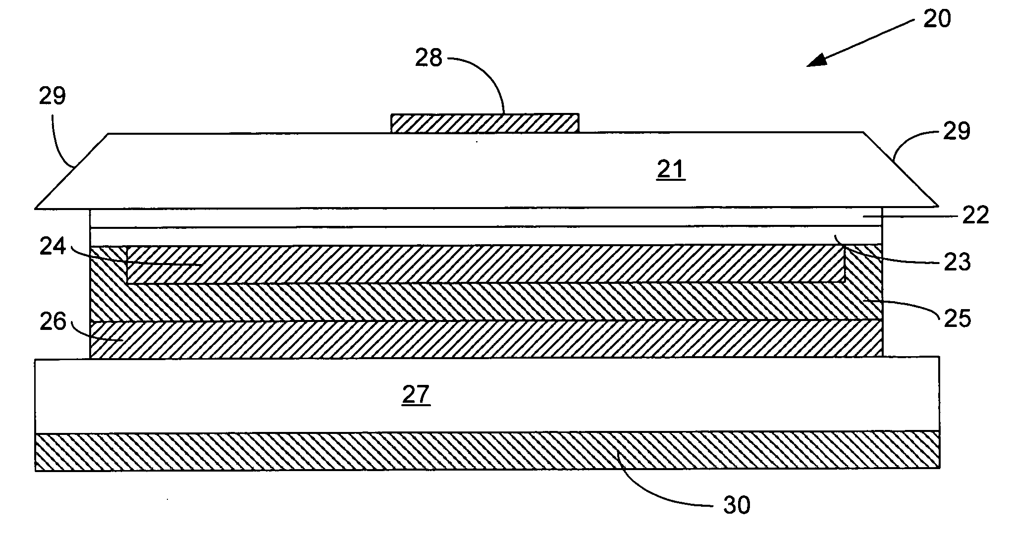
[0032]As further description, FIG. 1 is a cross sectional view of a light emitting diode broadly designated at 20 having the performance characteristics of the present invention. The diode 20 includes a transparent silicon carbide substrate 21 which is preferably a single crystal and has a polytype selected from the 3C, 4H, 6H, and 15R polytypes of silicon carbide with 4H often being preferred in the context of the present invention. Because FIG. 1 illustrates the diode 20 in the “flip chip” orientation (i.e., mounted for use with the active layers below the substrate), the substrate 21 appears at the top of the diode 20 rather tha...


PUM


Abstract

A light emitting diode is disclosed with advantageous output on a per unit area basis. The diode includes an area of less than 100,000 square microns, operates at a forward voltage of less than 4.0 volts, produces a radiant flux of at least 24 milliwatts at 20 milliamps drive current, and emits at a dominant wavelength between about 395 and 540 nanometers.

Description


Claims


Application Information

Patent Timeline
Owner CREELED INC
Learn More