
Implementing multipliers in a programmable integrated circuit device

Inactive Publication Date: 2013-06-18
ALTERA CORP
View PDF375 Cites 4 Cited by
  • Summary
  • Abstract
  • Description
  • Claims
  • Application Information

AI Technical Summary

Benefits of technology

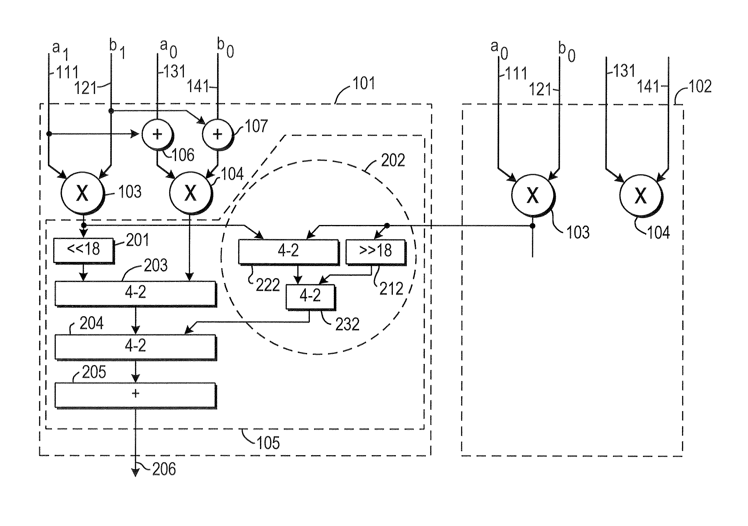
The present invention reduces the number of times we need to multiply numbers using large multipliers. For example, if we need to multiply two 36-bit numbers, we can use a technique to get the final result by adding the digits of each number and then multiplying them. This results in a combination of two products, which can then be added together. This method reduces the number of multipliers needed, which speeds up the process.

Problems solved by technology

As applications for which PLDs are used increase in complexity, it has become more common to design PLDs to include specialized processing blocks in addition to blocks of generic programmable logic resources.

Method used


Image

  • Implementing multipliers in a programmable integrated circuit device
  • Implementing multipliers in a programmable integrated circuit device
  • Implementing multipliers in a programmable integrated circuit device

Examples


Embodiment Construction

[0020]When a 36-bit-by-36-bit multiplication is implemented in 18-bit-by-18-bit multipliers using a linear decomposition, each of the two 36-bit operands a and b can be expressed as a set of two 18-bit numbers a1:a0 and b1:b0, so that their product M can be represented as follows:

M=(2xa1+a0)*(2xb1+b0)

The power-of-2 factors represent left-shifting by a number of places equal to the exponent. Expanding, the 36-bit-by-36-bit multiplication M is:

M=2xa1b1+2x(a1b0+a0b1)+a0b0

There are four unique terms anbm, so four multipliers are required.

[0021]Instead, however, in a recursive decomposition, such as the “Karatsuba multiplication” described, e.g., in Weisstein, E. W., “Karatsuba Multiplication,”MathWorld—A Wolfram Web Resource, http: / / mathworld.wolfram.com / KaratsubaMultiplication.html, the 18-bit components an, bm can be combined as follows:

A=(a1+a0)*(b1+b0)=a1b1+a1b0+a0b1+a0b0

Substituting A into the linear decomposition:

M=22xa1b1+2x(A−a1b1+a0b0)+a0b0

[0022]In this formulation of the co...


PUM


Abstract

The number of multipliers of a particular size that are required to perform a multiplication larger than that size is reduced. In the example of a 36-bit-by-36-bit multiplication, the number of 18-bit-by-18-bit multipliers required may be reduced from four to three. This may be achieved by using recursive decomposition techniques. As discussed in more detail below, if for each of two 36-bit numbers, the “digits” of each respective 36-bit number are added together, and then the two sums are multiplied, the resulting term can be combined additively with the product of the least-significant group of bits of the two 36-bit numbers and the product of the most-significant group of bits of the two 36-bit numbers to provide the desired product. A specialized processing block includes structures to facilitate the recursive decomposition technique.

Description

BACKGROUND OF THE INVENTION[0001]This invention relates to multiplication operations in programmable integrated circuit devices such as, e.g., programmable logic devices (PLDs).[0002]As applications for which PLDs are used increase in complexity, it has become more common to design PLDs to include specialized processing blocks in addition to blocks of generic programmable logic resources. Such specialized processing blocks may include a concentration of circuitry on a PLD that has been partly or fully hardwired to perform one or more specific tasks, such as a logical or a mathematical operation. A specialized processing block may also contain one or more specialized structures, such as an array of configurable memory elements. Examples of structures that are commonly implemented in such specialized processing blocks include: multipliers, arithmetic logic units (ALUs), barrel-shifters, various memory elements (such as FIFO / LIFO / SIPO / RAM / ROM / CAM blocks and register files), AND / NAND / OR...

Claims


Application Information

Patent Timeline
IPC IPC(8): G06F7/52
CPCG06F7/5324
Inventor LANGHAMMER, MARTIN
Owner ALTERA CORP
Learn More