
Image sensor comprising a waveguide structure and imaging apparatus

a waveguide structure and image sensor technology, applied in the field of image sensors and imaging apparatuses, can solve the problems of difficult to ensure the required mechanical strength of the insulating layer 3 and the difficulty of ensuring the required mechanical strength of the insulating layer, and achieve the effect of suppressing a reduction in the mechanical strength of the waveguide structure and improving the ratio of ligh

Active Publication Date: 2012-12-18
CANON KK
View PDF5 Cites 2 Cited by
  • Summary
  • Abstract
  • Description
  • Claims
  • Application Information

AI Technical Summary

Benefits of technology

[0013]The present invention provides for improving an ratio of a amount of light reaching a photoelectric conversion unit to an amount of light incident on a pixel while suppressing a reduction in a mechanical strength of a waveguide structure.
[0018]The present invention can improve the ratio of the amount of light reaching the photoelectric conversion unit to the amount of light incident on the pixel while suppressing a reduction in the mechanical strength of the waveguide structure.

Problems solved by technology

With this configuration, if the insulating layer 3 is formed of a material that has a refractive index sufficiently lower than that of the material 13, it may be difficult to ensure a required mechanical strength of the insulating layer 3 when a material with a sufficiently low refractive index has low mechanical strength.
However, in this case, it may be difficult to ensure the required mechanical strength of the insulating layer 3.

Method used


Image

  • Image sensor comprising a waveguide structure and imaging apparatus
  • Image sensor comprising a waveguide structure and imaging apparatus
  • Image sensor comprising a waveguide structure and imaging apparatus

Examples


Embodiment Construction

[0028]In the specification of the present invention, the term “incident angle” is defined as shown in FIG. 6. An angle of incident light strict perpendicular to a light receiving surface AS of an imaging device (i.e. an image sensor) shall be zero degrees. An angle of incident light in any arbitrary plane that is perpendicular to the light receiving surface AS of an imaging device can be positive or negative, as illustrated in FIG. 6. What the incident angle is large means that an absolute value of the incident angle is large. What the incident angle is small means that an absolute value of the incident angle is small. That is, a large incident angle indicates a large absolute value of the angle of incident light, and a small incident angle indicates a small absolute value of the angle of incident light.

[0029]Also, in the specification of the present invention, the term “light utilization efficiency” refers to a ratio of an amount of light reaching a photoelectric conversion unit PD...


PUM


Abstract

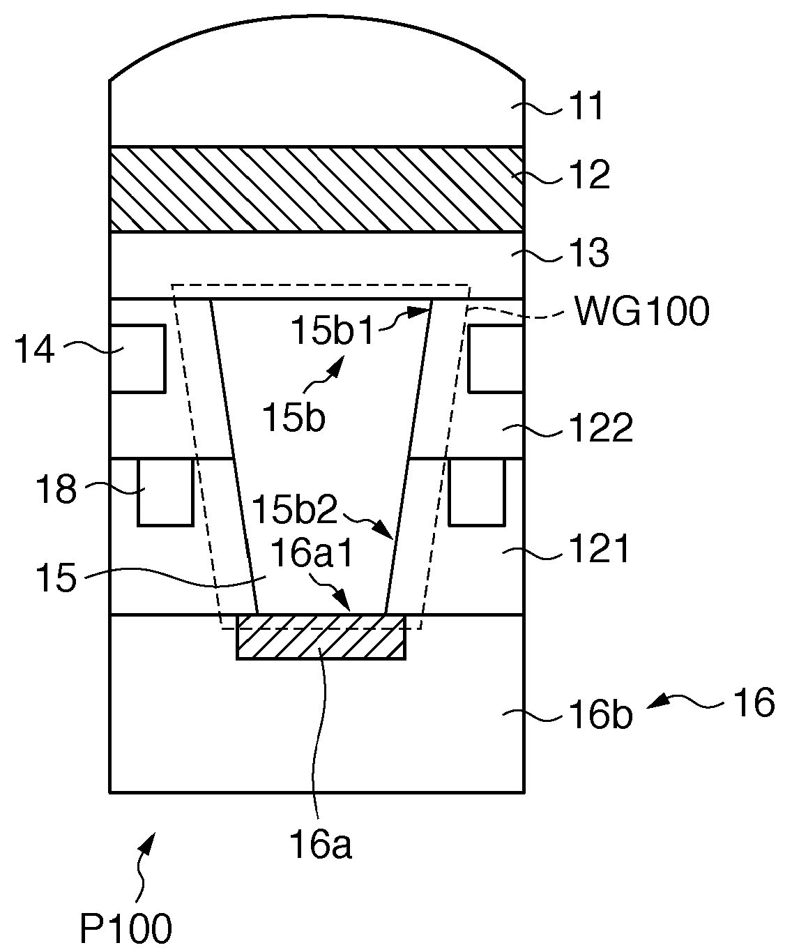
An image sensor includes a pixel array with a plurality of pixels, wherein each of the plurality of pixels includes: a photoelectric conversion unit; and a waveguide structure in which a side face of a substance that has a higher refractive index than a refractive index of a plurality of insulation films is surrounded by the plurality of insulation films so that light is guided to the photoelectric conversion unit, and wherein an insulation film that surrounds a region where the light is concentrated of the side face of the substance has the lowest refractive index among the plurality of insulation films.

Description

BACKGROUND OF THE INVENTION[0001]1. Field of the Invention[0002]The present invention relates to an image sensor and an imaging apparatus.[0003]2. Description of the Related Art[0004]Image sensors such as CCD image sensors and CMOS image sensors include a one- or two-dimensional pixel array with a plurality of pixels. In recent years, the number of pixels in the pixel array of an image sensor has increased in order to capture high-definition images. Some image sensors for use in imaging apparatuses, such as digital video cameras or digital still cameras, now have as many as several million pixels or more in their pixel arrays.[0005]Each pixel in a pixel array generates an image signal when incident light reaches a light receiving surface of a photodiode and the photodiode photoelectrically converts the received light. Thus, it is important to efficiently guide the light incident on a pixel to a photodiode in the pixel. In other words, assuming that “light utilization efficiency” is ...

Claims


Application Information

Patent Timeline
Patent Type & Authority Patents(United States)
IPC IPC(8): G02B27/10H01L27/14H04N5/335H04N5/369H04N101/00
CPCH01L27/14625H01L27/14629H01L27/14632H04N23/00H04N23/75
Inventor TAKUBO, YOUSUKEMIYAZAWA, SEIICHI
Owner CANON KK
Learn More